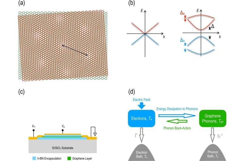
Moiré superlattice of graphene/h-BN. a Schematic showing the formation of a Moiré pattern in a heterostructure of two honeycomb crystals with similar lattice constants and a small rotational misalignment. The black arrow denotes the period of the resulting Moiré superlattice. b Schematics of the energy bands of monolayer graphene (left) and a graphene/h-BN heterostructure (right). The linear bands observed near the K-point in the monolayer are dramatically modified for the heterostructure, with inequivalent gaps appearing at the original Dirac point (Δ) and in the conduction (Δe) and valence (Δh) bands. c Schematic illustration of the transistor geometry utilized in our studies. Monolayer graphene is fully encapsulated between thick layers of h-BN and contacted with lithographically designed edge contacts. A top-gate is biased at a variable voltage (Vg) to sweep the Fermi level through the bands of (b). The pulsed voltage (Vin) is applied to the input signal line of a coplanar waveguide and the transistor current is measured by feeding it into the 50-Ω input of a fast oscilloscope. d The essential elements of our self-consistent theoretical model for electron–phonon energy exchange in graphene. Under non-equilibrium conditions, the electrons and phonons in graphene attain respective temperatures Te and Tph, determined by the strength of the electron–phonon coupling and the loss rates Γ and τp−1 to electron and phonon reservoirs, respectively. These reservoirs can be taken to be held at some common (fixed) equilibrium temperature (To). Credit: Nature Communications (2023). DOI: 10.1038/s41467-023-37292-4
Moiré patterns occur everywhere. They are created by layering two similar but not identical geometric designs. A common example is the pattern that sometimes emerges when viewing a chain-link fence through a second chain-link fence.
For more than 10 years, scientists have been experimenting with the moiré pattern that emerges when a sheet of graphene is placed between two sheets of boron nitride. The resulting moiré pattern has shown tantalizing effects that could vastly improve semiconductor chips that are used to power everything from computers to cars.
A new study led by University at Buffalo researchers, and published in Nature Communications, demonstrated that graphene can live up to its promise in this context.
"Our recent work shows that this particular sandwich of graphene and boron nitride elicits properties that are suitable for use in new technological applications," said Jonathan Bird, Ph.D., professor and chair of the Department of Electrical Engineering at UB.
Graphene is made of carbon, just like charcoal and diamonds. What distinguishes graphene is the way the carbon atoms are put together: they are linked in a hexagonal or honeycomb pattern. The resulting material is the thinnest material known to exist, so thin that scientists call it two-dimensional.
Left alone, graphene conducts electricity well—too well, in fact, to be useful in microelectronic technology. But by sandwiching graphene between two layers of boron nitride, which also has a hexagonal pattern, a moiré pattern results. The presence of this pattern is accompanied by dramatic changes in the properties of the graphene, essentially turning what would normally be a conducting material into one with (semiconductor-like) properties that are more amenable to use in advanced microelectronics.
This research establishes how the moiré pattern in graphene can be adapted to use in technological applications such as new types of communication devices, lasers and light-emitting diodes. "Our work demonstrated the viability of this approach, showing that the graphene/boron nitride sandwich that we are studying does indeed have the favorable properties needed for microelectronics," said Bird.
The semiconductor chips in question are essential not just in smartphones and medical devices but also in smart-home gadgets such as dishwashers, vacuums, and home-security systems. "Modern technology relies on the semiconductor chips that form the heart of their systems and control their operation," said Bird. "When you talk into your cell phone, it's the chip that converts your voice to an electronic signal and transmits it to a tower."
The graphene/boron-nitride heterostructure appears to have properties that are amenable to engineering. Developing future technology based on these materials may depend on discovering and harnessing properties that allow for greater speed and functionality. Bird noted that there is typically a lag between a discovery, the excitement about a discovery, and realizing the promise of the discovery. Graphene—so common that it's in any note scribbled with pencil—wasn't discovered until 2004.
Bird earned a Ph.D. in physics, but he was drawn to electrical engineering because it allowed him to explore quantum physics through research on semiconductors. Quantum physics—"the kind of magical physics that occurs at the atomic scale," he explained—can be observed through experiments using technology that explores material and processes at the atomic level.
"We can get a system to respond to actions we take, and that response reflects details of the atomic and quantum nature of the system," he said. Graphene attracted his attention because it appeared to be a way to study quantum effects through work on semiconductors. At UB, he established a lab called NoMaD, where he, his colleagues, and their students study "quantum phenomena occurring at the nanoscale." Graduates have gone on to careers at Intel and IBM as well as other universities.
In this research, Bird and his team have explored the properties of graphene within a certain limit that must be achieved to create new technologies. The semiconductor chip industry is a massive industry that continues to grow, demanding new materials, new ways to use existing materials, and a new workforce capable of developing both.
More information: Jubin Nathawat et al, Signatures of hot carriers and hot phonons in the re-entrant metallic and semiconducting states of Moiré-gapped graphene, Nature Communications (2023). DOI: 10.1038/s41467-023-37292-4
Journal information: Nature Communications
Provided by University at Buffalo


