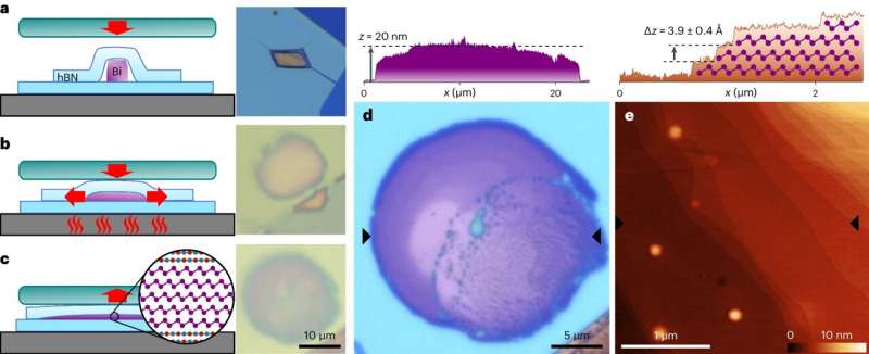
Growth of ultrathin bismuth crystals inside a vdW mold. a–c, Cross-sectional schematics of the vdW-mold process with corresponding optical images of the bismuth. a, Bismuth flake encapsulated in hBN on a bottom substrate of Si/SiO2 before squeezing. b, Uniaxial compression (vertical red arrow) is applied to the stack by a rigid top substrate (glass or sapphire) while the stage is heated. When the bismuth reaches its melting point, it rapidly compresses and expands laterally. c, Bismuth is cooled below its melting point and then pressure is removed, resulting in an ultrathin bismuth crystal. The inset shows the atomic structure. d, Optical image of the encapsulated vdW-molded bismuth (sample M30); black triangles indicate location of the AFM line trace (top) of the bismuth taken after removing the top hBN flake. This bismuth varies from 10 to 20 nm thick. e, AFM topography of the vdW-molded bismuth after removing the top hBN, showing wide flat terraces. Black triangles show location of the line trace (top). The average step height is 3.9 ± 0.4 Å. The diagram inset in the shaded region shows the crystal structure. Credit: Nature Materials (2024). DOI: 10.1038/s41563-024-01894-0
In a study published in Nature Materials, scientists from the University of California, Irvine describe a new method to make very thin crystals of the element bismuth—a process that may aid the manufacturing of cheap flexible electronics an everyday reality.
"Bismuth has fascinated scientists for over a hundred years due to its low melting point and unique electronic properties," said Javier Sanchez-Yamagishi, assistant professor of physics & astronomy at UC Irvine and a co-author of the study. "We developed a new method to make very thin crystals of materials such as bismuth, and in the process reveal hidden electronic behaviors of the metal's surfaces."
The bismuth sheets the team made are only a few nanometers thick. Sanchez-Yamagishi explained how theorists have predicted that bismuth contains special electronic states allowing it to become magnetic when electricity flows through it—something essential for quantum electronic devices based on the magnetic spin of electrons.
One of the hidden behaviors observed by the team is so-called quantum oscillations originating from the surfaces of the crystals.
"Quantum oscillations arise from the motion of an electron in a magnetic field," said Laisi Chen, a Ph.D. candidate in physics & astronomy at UC Irvine and one of the lead authors of the paper. "If the electron can complete a full orbit around a magnetic field, it can exhibit effects that are important for the performance of electronics. Quantum oscillations were first discovered in bismuth in the 1930s, but have never been seen in nanometer-thin bismuth crystals."
Amy Wu, a Ph.D. candidate in physics in Sanchez-Yamagishi's lab, likened the team's new method to a tortilla press. To make the ultra-thin sheets of bismuth, Wu explained, they had to squish bismuth between two hot plates. To make the sheets as flat as they are, they had to use molding plates that are perfectly smooth at the atomic level, meaning there are no microscopic divots or other imperfections on the surface.
"We then made a kind of quesadilla or panini where the bismuth is the cheesy filling and the tortillas are the atomically flat surfaces," said Wu.
"There was this nervous moment where we had spent over a year making these beautiful thin crystals, but we had no idea whether its electrical properties would be something extraordinary," said Sanchez-Yamagishi. "But when we cooled down the device in our lab, we were amazed to observe quantum oscillations, which have not been previously seen in thin bismuth films."
"Compression is a very common manufacturing technique used for making common household materials such as aluminum foil, but is not commonly used for making electronic materials like those in your computers," Sanchez-Yamagishi added. "We believe our method will generalize to other materials, such as tin, selenium, tellurium and related alloys with low melting points, and it could be interesting to explore for future flexible electronic circuits."
Next, the team wants to explore other ways in which compression and injection molding methods can be used to make the next computer chips for phones or tablets.
"Our new team members bring exciting ideas to this project, and we're working on new techniques to gain further control over the shape and thickness of the grown bismuth crystals," said Chen. "This will simplify how we fabricate devices, and take it one step closer for mass production."
The research team included collaborators from UC Irvine, Los Alamos National Laboratory and the National Institute for Materials Science in Japan.
More information: Laisi Chen et al, Exceptional electronic transport and quantum oscillations in thin bismuth crystals grown inside van der Waals materials, Nature Materials (2024). DOI: 10.1038/s41563-024-01894-0
Journal information: Nature Materials
Provided by University of California, Irvine


