Credit: AI-generated image (disclaimer)
An international team of researchers from the National Physical Laboratory (NPL), IBM, the University of Edinburgh and Auburn University have shown that a new device concept - a 'squishy' transistor - can overcome the predicted power bottleneck caused by CMOS (complementary metal-oxide-semiconductor) technology reaching its fundamental limits.
Moore's law predicted that the number of transistors able to fit on a given die area would double every two years. As transistor density doubled, chip size shrank and processing speeds increased. This march of progress led to rapid advances in information technology and a surge in the number of interconnected devices. The challenge with making anything smaller is that there are fundamental physical limits that can't be ignored and we are now entering the final years of CMOS transistor shrinkage.
Furthermore, this proliferation is driving an increase in data volume, accompanied by rising demands on energy to process, store and communicate it all; as a result, IT infrastructure now draws an estimated 10 % of the world's electrical power. Previous efforts have focused on remediation by reducing the amount of energy per bit. However, soon we will hit a power barrier that will prevent continued voltage scaling. The development of novel, low-power devices based on different physical principles is therefore crucial to the continued evolution of IT.
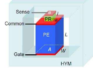
A team from NPL, IBM, Edinburgh and Auburn have demonstrated the capabilities of the Piezoelectric Transistor (PET) as a post-CMOS technology that could overcome these issues and restore voltage scaling. In the paper, published in Applied Physics Letters, the team explain the physics underlying the PET's behaviour and use theory and simulation to predict its performance when optimised across a wide range of application spaces, spanning several different length scales: including radio frequency switches (on the micron scale) and devices such a smartphones and phased array radar.
Schematic of the PET
The conceptual device is based on a pressure-driven insulator-to-metal transition, and has proved to be a promising, fast, low-power option for future IT infrastructure, with a performance that cannot be matched by CMOS transistors. These results should spur further research into piezoelectric scaling, and the PET fabrication techniques needed to realise this device in the future.
More information: "The piezoelectronic stress transduction switch for very large-scale integration, low voltage sensor computation, and radio frequency applications." Appl. Phys. Lett. 107, 073505 (2015); dx.doi.org/10.1063/1.4928681
Journal information: Applied Physics Letters
Provided by National Physical Laboratory


