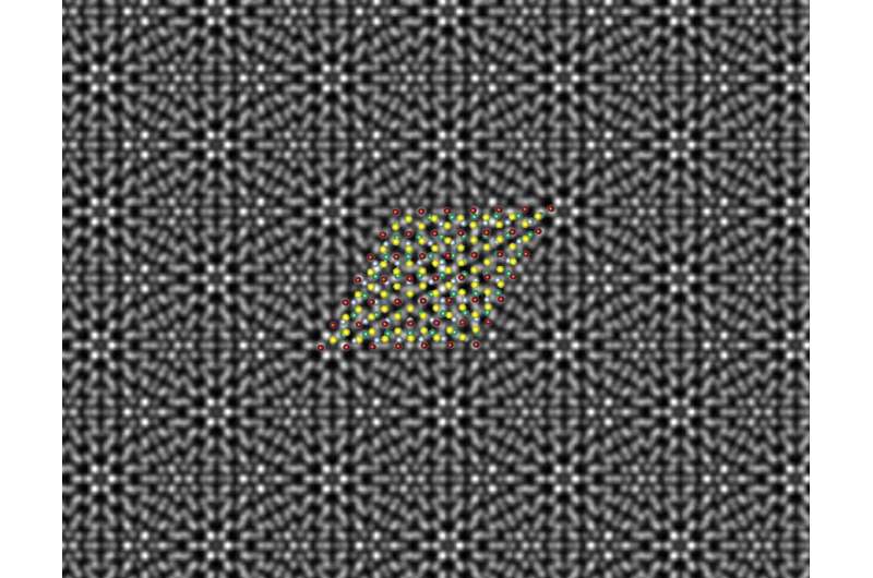
A scanning transmission electron microscope image reveals a beautiful periodic pattern (called a “moiré pattern") resulting from the epitaxial chromium telluride/tungsten diselenide superlattice; superimposed is the atomic model of the superlattice. Credit: Mengying Bian and Liang Zhu
Scientists have grown thin films of two different crystalline materials on top of each other using an innovative technique called "dative epitaxy." The researchers discovered the method by surprise.
As University at Buffalo physicist Hao Zeng explains, dative epitaxy holds layers of different materials together via a weak attractive force between the materials, paired with occasional chemical bonds called "dative bonds."
"I compare this to laying down wood floor in your home," says Zeng, professor of physics in the UB College of Arts and Sciences. "You put a few nails in to anchor the wood planks on the surface. The dative bonds are like these nails."
The research is exciting, Zeng says, because new ways to layer films "could have far-reaching impacts in the fields of semiconductors, quantum technology and renewable energy."
Zeng and colleagues report on dative epitaxy in a March paper in Advanced Materials.
A 'fortuitous' discovery
"We did not start with the idea of dative epitaxy," Zeng says. "I would say it was a fortuitous discovery. Initially, we were trying to grow atomically thin magnets on a layer of van der Waals material, which acts as a template to promote 2D growth."
As part of this magnet-making, Bian, a UB physics postdoctoral researcher, grew a super-thin layer of chromium telluride atop a super-thin "monolayer" of tungsten diselenide.
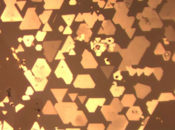
A microscope image shows numerous super-thin chromium telluride crystals grown atop tungsten diselenide. The crystals' neat alignment with one another is an indication of dative epitaxy, the method through which the crystals were grown. Credit: Mengying Bian
The scientists thought the two films would be held together only by a weak attraction between the materials, known as the van der Waals force. But a peek under the microscope revealed something unexpected.
"When Mengying came into the office and showed me this very nice microscope image, we immediately realized there was something unusual," Zeng recalls. "The crystals looked like they were perfectly aligned with each other, and this kind of perfect alignment suggested that it might not be the van der Waals epitaxy we were expecting. In van der Waals epitaxy, the orientation of layers cannot be controlled very accurately because the layers are not strongly interacting with each other."
After further experimental and theoretical analysis, in collaboration with Renat Sabirianov, Ph.D., at the University of Nebraska at Omaha, the researchers concluded that in addition to the van der Waals force, "sporadic" dative bonds connected the two films.
Then came another surprise. When Zeng searched for existing literature on dative epitaxy, he found only one: a recent theoretical work predicting dative bond enhanced van der Waals epitaxy. The study was led—again, serendipitously—by his long-time collaborator at Rensselaer Polytechnic Institute, Shengbai Zhang, Ph.D. Zhang "was very excited to hear that our experimental discovery verified his hypothesis," Zeng says.
'Goldilocks principle' of epitaxy
UB has filed a provisional patent application for dative epitaxy methods, and is looking to expand on this research through collaboration with industry and research partners. Zeng and Bian say the technique represents a "Goldilocks principle" when it comes to layering crystalline films.
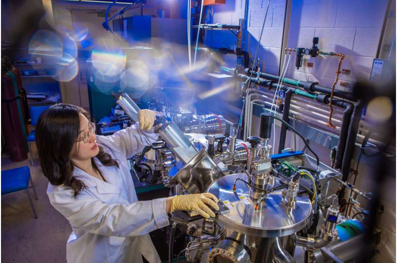
UB physics postdoctoral researcher Mengying Bian works with a dual chamber thin film deposition system. Credit: Douglas Levere / University at Buffalo
Epitaxy involves growing one crystalline material on another crystalline substrate, with a well-defined orientation relationship between them. Conventional epitaxy requires that two materials share similar lattice spacing, which has to do with the distance between atoms. Van der Waals epitaxy overcomes this hurdle but can lead to crystals growing in the wrong direction.
"Dative epitaxy circumvents the stringent lattice-matching requirements in conventional epitaxy, while also taking advantage of the formation of special chemical bonds to fix crystal orientation," Bian says.
"Dative epitaxy could allow a broader range of materials to be grown. It really gives people a lot of flexibility and choice," Zeng says. "It's the Goldilocks principle in epitaxy: It captures the benefits of conventional and van der Waals epitaxial techniques, but addresses the drawbacks of both."
Given these advantages, Zeng says, their "technique could open the door to high-quality epitaxial growth of a variety of compound semiconductor thin films, such as, potentially, gallium arsenide or gallium nitride on silicon wafers. Integrating these materials are super important to the semiconductor industry, which has been a longstanding challenge due to the limitations of other forms of epitaxy."
More information: Mengying Bian et al, Dative Epitaxy of Commensurate Monocrystalline Covalent van der Waals Moiré Supercrystal, Advanced Materials (2022). DOI: 10.1002/adma.202200117
Journal information: Advanced Materials
Provided by University at Buffalo


