Small-area, low-power, low-noise instrumentation amplifiers (IA) are critical components of arrayed sensor devices used for high-spatial-resolution biomedical and environment monitoring system.
However, in order to realize small offset voltages of IA, conventional IAs utilize analog filters—composed of large passive components, resistors and capacitors— resulting in excessively large silicon chips.
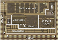
Now, Ippei Akita and colleague at Toyohashi University of Technology have developed a novel architecture for fabricating smaller sized integrated circuit chips. The technique is based on a digital calibration scheme for minimizing the offset voltage of the IA circuit, instead of an analog scheme used in conventional circuits.
The offset exists mainly at the first-stage circuit of IA. In this design, the researchers introduced a reconfigurable first-stage circuit. The best configuration for minimizing the offset was easily determined by calibration logic which was implemented in a small area compared to analog circuits.
The proposed IA was implemented in a standard 0.18 micrometer CMOS and resulted with an offset voltage of < 3.5 μV while drawing a current of 194 μA. The active area of the IA is 7.8 times smaller than conventional state-of-the-art chips while maintaining low noise and low power.
The researchers plan to use the proposed IA for the fabrication of an arrayed IA for high-spatial-resolution and real-time sensing systems.
More information: Akita, I. and Ishida, M. A 0.06mm2 14nV/√Hz chopper instrumentation amplifier with automatic differential-pair matching. IEEE Int. Solid-State Circuits Conf. Dig. Tech. Papers (ISSCC), pp.178-179, Feb. 2013.
Provided by Toyohashi University of Technology


