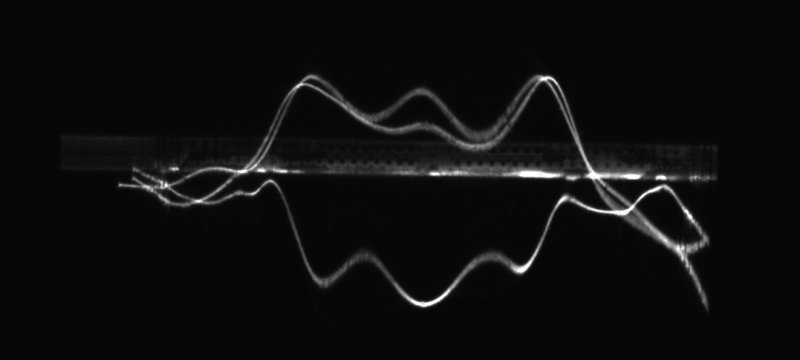
Novel technique measures warpage in next-gen integrated circuits

As integrated circuit components are coming up against size limits, manufacturers are turning to new approaches based on stacking extremely thin wafers. However, the thin wafers easily warp under the stresses involved in fabrication, and measuring the stress and warpage has so far proven challenging.
In a paper published in the Journal of Applied Crystallography, Professor Patrick McNally's team at Dublin City University, together with collaborators Brian Tanner at Durham University and Andreas Danilewsky at the University of Freiburg, report on a new technique using the Test beamline (B16) at Diamond Light Source to accurately, precisely, and verifiably measure the stress and warpage in individual silicon wafers. The researchers are now cooperating with industry partners to translate their approach into a tool which can be used for quality assurance and to improve fabrication processes. Meanwhile, they continue to work at Diamond to improve the technique and adapt it to different contexts and materials.
A stack of measurement trouble
In a 1965 paper, Intel co-founder Gordon Moore observed that the density of transistors in integrated circuits doubled every 18-24 months, a trend which has held well in the decades since. However, manufacturing techniques are nearing the limits of 'Moore's law' as the components printed onto integrated circuits approach atomic dimensions. To continue improving performance, manufacturers are exploring a new direction by combining different chips, each with a specialised function, into a vertical package in a 'more than Moore' approach known as heterogeneous integration.
The new technique involves using wafers less than a tenth as thick as those currently in use. Since they are so thin – just 25 to 100 µm – the wafers are extremely flexible, but they are also subjected to extreme stress during the fabrication process. "Imagine you glue together four or five pieces of silicon, each thinner than a human hair, then heat them up to 100-200° C, and then stand on top of them with your boot. Maybe you jump up and down a bit. That's the sort of damage that's done as part of semiconductor processing," explains Professor Patrick McNally of Dublin City University. The stress and resulting warpage of the wafers during manufacturing can lead to malfunctions, altered performance, and silicon 'real estate' lost to stress-related 'keep out zones' on the chip. To avoid these pitfalls, manufacturers are eager to understand how to manage stress and warpage in their design and fabrication processes.
So far, measuring the warpage of the individual silicon wafers without damaging them has been impossible, forcing people to use the warpage of the entire package as a proxy. Using the Test beamline (B16) at Diamond, the trio have developed a non-destructive technique to precisely and accurately measure the warpage of each wafer in a package through transmission X-ray diffraction imaging. To confirm their measurement technique, the team included samples with known curvature and displacement from IMEC in Belgium. "We've proven that it can be done reliably and verifiably," said Professor McNally.
To industry and beyond
While the new technique shows great promise, "no one in the semiconductor business is going to back a synchrotron into their fabrication facility," noted Professor McNally. The team has already successfully carried out preliminary trials with a commercial tool as an X-ray source, and work is underway with X-ray metrology companies to bring the technique into industry as a quality assurance tool. Improving the measurement speed of the commercial tools is a major outstanding challenge – measurements done in minutes at Diamond can take hours with commercial tools – but the team is pursuing avenues to improve this.
The technique offers an opportunity not only to measure warpage during fabrication but also to improve the design process. Mechanical engineers at a large chip company are working with the team to test the finite element models they use to predict stress and warpage in their designs. "The idea is that we provide a 'sanity check' on their modelling so they can use it to improve their designs," said Professor McNally.
Meanwhile, the team is continuing to develop the approach using the facilities at Diamond, which underpins any advancements. The team has recently tested their new technique on chips, which were receiving power to measure how the warpage might change under different usage conditions. "We do our top end development at Diamond," said Professor McNally, explaining that the ability to rapidly test and explore ideas at the synchrotron is crucial before they can be adapted for industry applications.
More information: B. K. Tanner et al. Nondestructive X-ray diffraction measurement of warpage in silicon dies embedded in integrated circuit packages, Journal of Applied Crystallography (2017). DOI: 10.1107/S1600576717003132
Provided by Diamond Light Source


