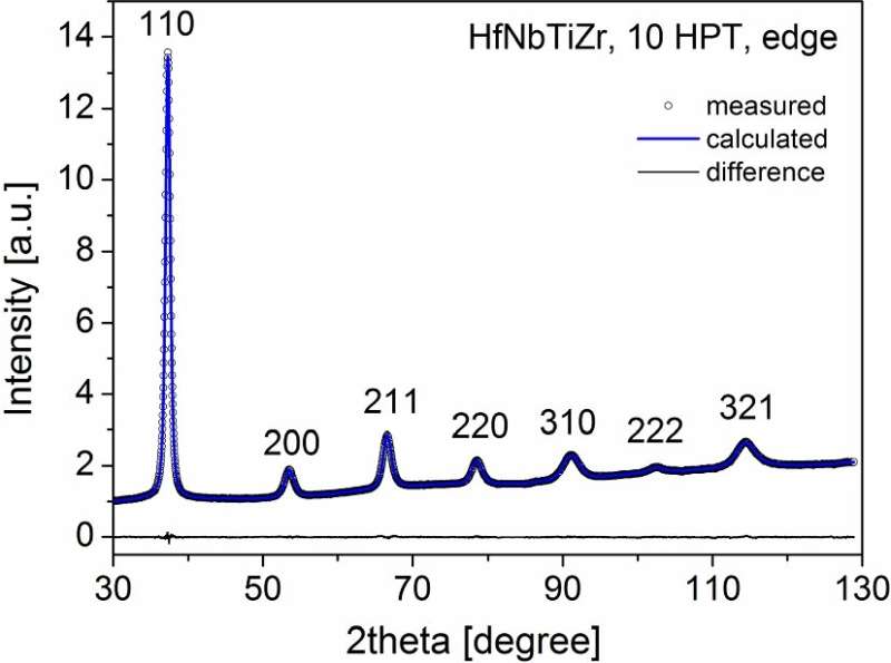
Whole diffraction pattern fitting on a nanocrystalline HfNbTiZr MPEA processed by ten turns of HPT using the CMWP evaluation method. Credit: The European Physical Journal Special Topics DOI: 10.1140/epjs/s11734-022-00572-z
Owing to their unique physical properties, nanostructured materials are now at the forefront of materials science. Several different techniques can be used to characterize their microscopic features, but each of these has its pros and cons. In new research published in The European Physical Journal Special Topics, Jenő Gubicza at ELTE Eötvös Loránd University, Budapest, shows that one indirect method, named X-ray diffraction line profile analysis (XLPA) is suitable for analyzing nanostructured materials, but its application and interpretation require special care for obtaining reliable conclusions.
Nanostructured materials consist of nanoscale grains, each composed of an orderly atomic lattice. Useful properties stem from abrupt changes to the arrangements of atoms in these lattices, named "defects." To fine-tune a nanostructure's material properties, researchers can control the density of these defects by an appropriate selection of the processing conditions of nanomaterials.
To compare the defect densities introduced by both of these approaches, XLPA measures how X-rays are diffracted by the microstructures contained in the materials as they pass through. The concern here is whether the information about defect structure obtained by XLPA is reliable, since this method studies the material indirectly only through the scattering of X-rays. Alternatively, transmission electron microscopy (TEM) can provide extensively detailed images of these microstructures, but can only be used to study tiny volumes.
In his analysis, Gubicza compares the microstructures determined indirectly through XLPA, with those obtained directly through TEM. On the one hand, he found that the defect densities determined by the two methods agree well. On the other, while the grain size measured by both techniques tend to diverge in materials with larger grain sizes, they largely agreed with each other for grain sizes smaller than 20 nanometers. In these cases, XLPA correctly showed that both top-down and bottom-up processing methods of nanomaterials can produce similarly high defect densities. Altogether, Gubicza's overview provides researchers with useful guidance on how and when XLPA should be applied.
More information: Jenő Gubicza, Reliability and interpretation of the microstructural parameters determined by X-ray line profile analysis for nanostructured materials, The European Physical Journal Special Topics (2022). DOI: 10.1140/epjs/s11734-022-00572-z
Provided by Springer


