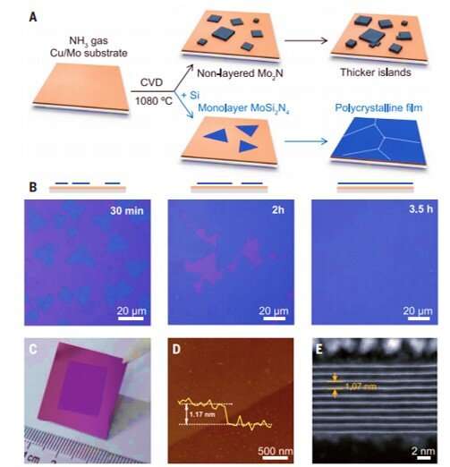
Chemical vapor deposition growth of MoSi2N4. (A) Schematic of two CVD growth processes, showing that layered MoSi2N4 is formed by simply adding Si during the growth of nonlayered 2D Mo2N. (B) Optical images of MoSi2N4 grown by CVD for 30 min, 2 hours, and 3.5 hours, illustrating the formation process of a monolayer MoSi2N4 film (schematic shown at top). The samples were transferred onto SiO2/Si substrates. (C) Photograph of a CVD-grown 15 mm × 15 mm MoSi2N4 film transferred onto a SiO2/Si substrate. (D) A typical AFM image of MoSi2N4 film, showing thickness of ~1.17 nm. (E) Cross-sectional HAADF-STEM image of a thick MoSi2N4 domain, showing a layered structure with an interlayer spacing of ~1.07 nm. Credit: Science Advances, doi: 10.1126/science.abb7023
In a new report published in Science, Yi-Lun Hong and a group of research scientists in materials science, engineering, and advanced technology in China and the U.K. investigated two-dimensional (2-D) materials to discover new phenomena and unusual properties. The team introduced elemental silicon during chemical vapor deposition-based growth of molybdenum nitride to passivate its surface and develop centimeter-scale, monolayer nitride films with silicon such as MoSi2N4. They built the monolayer film with seven atomic layers in the order of nitrogen-silicon-nitrogen-molybdenum-nitrogen-silicon-nitrogen (N-Si-N-Mo-N-Si-N), and the resulting material showed semiconducting behavior and excellent stability under ambient conditions. Using density functional theory (DFT) calculations, the scientists predicted a large family of such monolayer structured 2-D materials to exist with useful applications as semiconductors, metals and magnetic half-metals.
Two-dimensional materials
Two-dimensional materials have attractive properties that are suited for a variety of technical applications. Of these, transition metal carbides and nitrides (TMCs and TMNs) can form a large family of non-layered materials to combine properties of ceramics and metals. The MAX phase, where M stands for an early transition metal, A is an A-group element such as aluminum or silicon and X is carbon, nitrogen or both, forms the basis for monolayer MXenes. Such monolayer films can be selectively synthesized by etching the A-element layer. These materials have a hydrophilic (water-loving) surface and high electrical conductivity with promising applications including energy storage, sensors and catalysis. Scientists have recently developed a chemical vapor deposition (CVD) method to grow high-quality, nonlayered 2-D TMC and TMN crystals with diverse structures. But the surface energy constraints caused the nonlayered materials to grow as islands instead of layers. In this work, Hong et al. therefore grew 2-D molybdenum nitride and the MoSi2N4 compound using chemical vapor deposition.
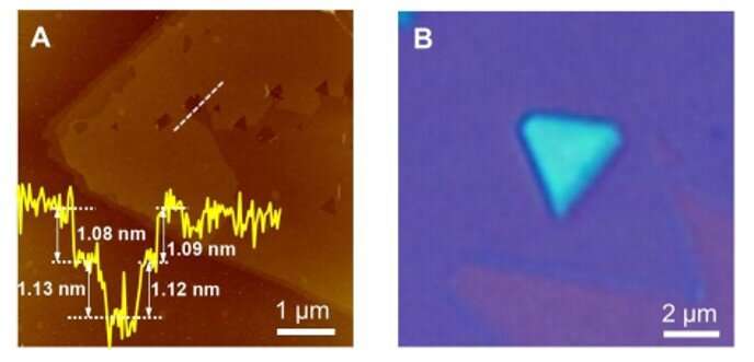
Thick MoSi2N4 domains synthesized with a higher feeding rate of ammonia (NH3) gas. (A) Atomic force microscopy (AFM) image of a non-uniform thick MoSi2N4 domain, showing steps with uniform height of ~1.1 nm. (B) Optical image of a thick MoSi2N4 domain grown on monolayer surface. Credit: Science Advances, doi: 10.1126/science.abb7023
Developing and characterizing the newly formed 2-D materials
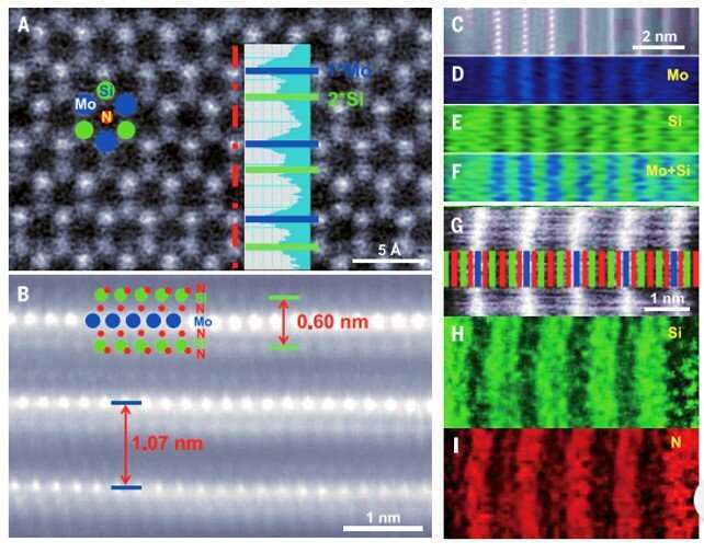
During the experiments, the scientists used a copper/molybdenum (Cu/Mo) bilayer as the substrate and ammonia (NH3) gas as the source of nitrogen. When they introduced elemental silicon to the experimental setup, the growth of the substrate markedly changed to form a uniform polycrystalline film. The team determined the thickness of the material surface using atomic force microscopy (AFM) and noted the surface growth process to be robust. Typically, the addition of an element to a growing 2-D material can only cause doping without changing the crystal structure of the matrix. But in this instance, adding silicon led to a new monolayered compound instead of simply doping the substrate. Hong et al. identified the crystal structure of the newly formed 2-D material using advanced transmission electron microscopy (TEM) and tested its surface elements using energy dispersive x-ray spectroscopy (EDS), electron energy-loss spectroscopy (EELS) and X-ray photoelectron spectroscopy (XPS).
DFT predictions of the MA2Z4 family. (A to C) Electronic band structure of (A) monolayer WSi2N4, (B) MoSi2As4, and (C) VSi2N4 calculated with PBE. In (C), the blue and red curves correspond to the spin-up and spin-down channels of the electronic band structure of the ferromagnetic ordering configuration, respectively. Credit: Science Advances, doi: 10.1126/science.abb7023
Confirming the MoSi2N4 formula and highlighting the material properties.
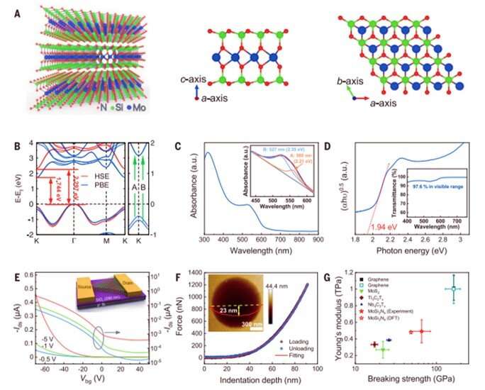
Since it was difficult to image the exact positions of nitrogen atoms using transmission electron microscopy, the team performed density functional theory (DFT) calculations of the compound to reveal its structural formula. The process confirmed the presence of a van der Waals (vdW) layered 2-D material containing the MoSi2N4 formula. Then using molecular dynamics calculations, they observed the structure to be dynamically and thermodynamically stable – while Raman spectra indicated high crystal quality of the MoSi2N4 structure. Using DFT calculations again, Hong et al noted the MoSi2N4 monolayer to maintain semiconductor properties (optical and electrical properties) alongside a carrier mobility that relied on the elastic modulus of the material.
Structural characterizations of MoSi2N4. (A) Plan-view high-angle annular dark field scanning transmission electron microscopy (HAADF-STEM) image of monolayer MoSi2N4. Inset is the intensity profile along the red dash-dot line, indicating that the bright dots are Mo atoms and the less bright dots are Si atoms. The image intensity is proportional to Z1.7 (where Z is atomic number). (B) Cross-sectional high-magnification HAADF-STEM image of multilayer MoSi2N4, showing a layered structure and Mo and Si atoms in each layer. The N atoms are marked according to the calculated structure. (C to F) Cross-sectional HAADF-STEM image (C) of a multilayer MoSi2N4, the corresponding high-resolution EDS mappings of Mo (D) and Si (E) elements, and mixed EDS mapping of Mo and Si elements (F). (G to I) Cross-sectional HAADF-STEM image (G) of a multilayer MoSi2N4, clearly showing the Mo layer, and the corresponding high-resolution EELS mapping of Si (H) and N (I) elements. The colored lines in (G) represent the positions of different elements (blue, Mo; green, Si; red, N). Credit: Science Advances, doi: 10.1126/science.abb7023
To study the optical properties of the monolayer MoSi2N4 film, Hu et al. transferred it onto a sapphire substrate and measured its bandgap, where the semiconducting monolayer maintained a high optical transmittance comparable to graphene. To test the electrical transport properties of the materials, Hong et al. fabricated back-gated field-effect transistor devices to observe typical semiconductor behavior. The scientists then measured the mechanical properties of the monolayer film using nanoindentation to highlight the elastic behavior of the membrane. The newly formed material showed long-term stability for handling, storage, and processing under ambient conditions without a protective environment in contrast to other materials.
Atomic structure, band structure, and optical, electrical, and mechanical properties of MoSi2N4. (A) The atomic model of MoSi2N4 with three layers (left) and the detailed cross-sectional (center) and in-plane (right) crystal structure of the monolayer. (B) Electronic band structure of monolayer MoSi2N4 calculated with PBE (blue lines) and HSE (red lines), respectively. Green arrows indicate two direct excitonic transitions at the K point, with the energy splitting originating from VB spin-orbit coupling. (C) Optical absorption spectrum of a monolayer MoSi2N4 film in the visible range. The inset shows that the peak at 500 to 600 nm can be fitted into two subpeaks, A (560 nm, 2.21 eV) and B (527 nm, 2.35 eV), corresponding to the two direct excitonic transitions in (B). (D) Tauc plot of a monolayer MoSi2N4 film. The inset shows the optical transmittance in the visible range. (E) Transfer characteristics of a monolayer MoSi2N4 BG-FET in linear scale (left axis, lower curves) and log scale (right axis, upper curves) measured at 77 K. Channel length, 30 mm. Inset: 3D schematic of a MoSi2N4-based BG-FET on a Si substrate with 290-nm SiO2. (F) A typical force-displacement curve of a single-crystal MoSi2N4 monolayer in AFM nanoindentation. The black, blue, and red lines are the loading, unloading, and fitting curves, respectively. Inset: AFM image of a suspended MoSi2N4 monolayer before indentation test; the height profile (red line) along the yellow dashed line shows an indentation of ~23 nm in the hole. (G) Comparison of Young’s modulus and breaking strength of monolayer MoSi2N4 with those of monolayer graphene, MoS2, and MXenes reported in the literature. All the strength values were derived according to the linear elastic model. The DFT-calculated modulus and strength of monolayer MoSi2N4 (open star) and the modulus and strength of monolayer graphene that we measured (open square) are also included. Credit: Science Advances, doi: 10.1126/science.abb7023
Creating a broad class of 2-D van der Waals (vdW) layered materials
Hong et al. showed how diverse transition metal elements could potentially replace the corresponding elements in MoSi2N4 based on additional DFT calculations to create a broad class of 2-D van der Waal layered materials with similar crystal structure. In this instance, they represented the materials with the general formula of MA2Z4, where M represented an early transition metal, A was silicon or Germanium and Z stood for nitrogen, phosphorous or arsenic. The elemental diversity in MA2Z4, allowed wide tunability of their bandgap and magnetic properties with applications in optoelectronics, electronics and spintronics. Using such materials, the scientists will be able to investigate hitherto unknown exciting properties and applications that exist within layered materials. In this way, the chemical vapor deposition method described here will pave the way to synthesize diverse materials in 2-D and monolayer forms.
More information: Hong Y. et al. Chemical vapor deposition of layered two-dimensional MoSi2N4 materials, Science Advances, 10.1126/science.abb7023
A. K. Geim et al. The rise of graphene, Nature Materials (2007). DOI: 10.1038/nmat1849
Wang Q. H. et al. Electronics and optoelectronics of two-dimensional transition metal dichalcogenides, Nature Nanotechnology, 10.1038/nnano.2012.205
Journal information: Science , Nature Materials
© 2020 Science X Network


