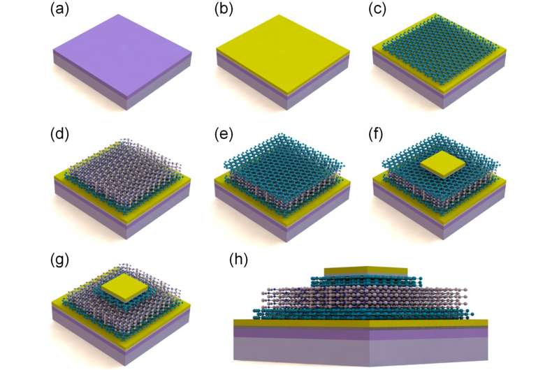
Resistive random access memory made of graphene electrodes and hexagonal boron nitride dielectric. Credit: Copyright American Institute of Physics 2017. Reproduced with permission from the authors.
Graphene and related two-dimensional (2-D) materials have raised massive interest and investment during the last years. However, the amount of 2-D materials-based commercial devices available in the market is still very low.
The research group led by Dr. Mario Lanza at Soochow University (China) is leading a global effort to investigate the properties of layered dielectrics. In their recent investigation, published in the journal 2-D Materials, Prof. Lanza and co-workers synthesized a resistive random access memory (RRAM) using graphene/hexagonal-boron-nitride/graphene (G/h-BN/G) van der Waals structures.
Furthermore, they developed a compact model to accurately describe its functioning. The model is based on the nonlinear Landauer approach for mesoscopic conductors, in this case, atomic-sized filaments formed within the 2-D materials system. Besides providing excellent overall fitting results (which have been corroborated in log-log, log-linear and linear-linear plots), the model is able to explain the dispersion of the data obtained from cycle to cycle in terms of the particular features of the filamentary paths, mainly their confinement potential barrier height.
The development of theoretical models to describe the functioning of electronic devices is one essential step enabling device/systems simulation, which is essential before device mass production. The device selected in this case, the RRAM device, is the most promising technology for future high-density information storage.
More information: Chengbin Pan et al. Model for multi-filamentary conduction in graphene/hexagonal-boron-nitride/graphene based resistive switching devices, 2D Materials (2017). DOI: 10.1088/2053-1583/aa7129
Provided by Lanzalab


