Credit: Qian Xuesen Laboratory of Space Technology
The realization of photonic chips is a long–sought research goal. Surface plasmon polariton devices and circuits, which bridge the gap between integrated photonics and microelectronic technologies, are promising candidates for on-chip ultracompact planar structures. Integrated wavelength demultiplexers, which can separate different incident light wavelengths to propagate in different channels, are an essential component of photonic chips, and have great potential applications for a variety of integrated plasmonic devices and circuits. However, to date, proposals for wavelength demultiplexers are very limited, and the existing devices operate only within a narrow band and the large device size is not suitable for integration.
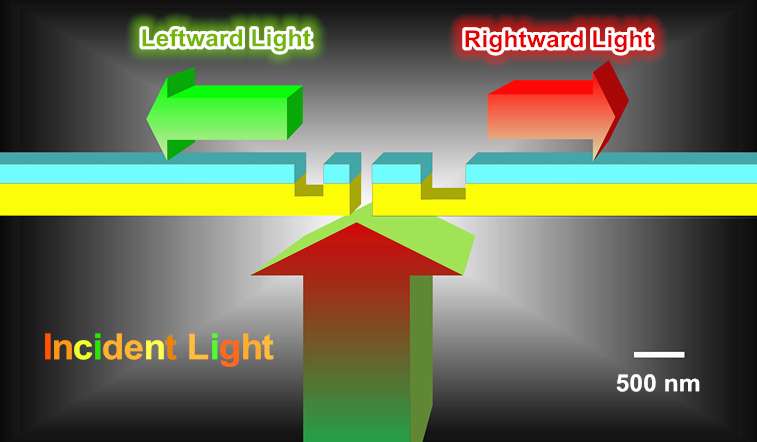
Recently, Chinese researchers have demonstrated a broadband and ultracompact nanoscale wavelength demultiplexer based on multi-component nano-cavities. This work has been published in the journal Scientific Reports.
In the past decade, researchers have developed two primary methods to realize wavelength demultiplexers. The first approach is designing different gratings based on Bragg reflection, but the bulky periodic configurations increase their sizes dramatically, limiting the integration of such architectures. The second approach is based on the optical interferences through etching asymmetric nano-slits or grooves directly on gold films. This approach ensures compact size, but the operation band is narrow and the contrast ratio is not high. In Lu's work, the authors designed and fabricated asymmetric muti-component nano-cavities. The unique dispersion properties and the low-quality factor of the multi-component nano-cavity guaranteed that the plasmonic wavelength demultiplexer operated in a broadband from 780 nm to 980 nm, which was enlarged by one order of magnitude compared with previous reports. The multi-component nano-cavity has strong confinement and modulation on the surface plasmon polariton, ensuring that the wavelength demultiplexer has an ultracompact size of only 2.3 μm. In addition, the intensity ratio of the demultiplexer has a maximum of 13.7 dB, which is among the highest values reported. Furthermore, the sample is easy to fabricate using a focused ion beam etching system.
"We have developed a theory and constructed a formula to describe multi-component nano-cavities. The multi-component nano-cavity configuration guarantees broadband operation and ultra-small size for the device. This provides a general guide for the design of the device," said Yong-Chun Liu, the second author of the paper, an expert on micro-cavity and quantum-optics.
The device with planar configuration is easy to fabricate and suitable for practical on-chip integration applications. This broadband plasmonic wavelength demultiplexer may have promise in optical communications, relying on structures that collect and sort photons by wavelength. This work provides a basis for the construction of on-chip photon routers, and also has potential applications for chip-integrated filters and all-optical logic gates.
Professor Lu has expertise in integrated all-optical devices, including all-optical logic discriminators all-optical logic comparators, and all-optical control of the slow light effect. "We are doing further research on more functional nanoscale photonic devices and we hope to realize an all-optical chip in future," said Prof. Lu.
More information: Cuicui Lu et al. Integrated ultracompact and broadband wavelength demultiplexer based on multi-component nano-cavities, Scientific Reports (2016). DOI: 10.1038/srep27428
Journal information: Scientific Reports
Provided by Qian Xuesen Laboratory of Space Technology


