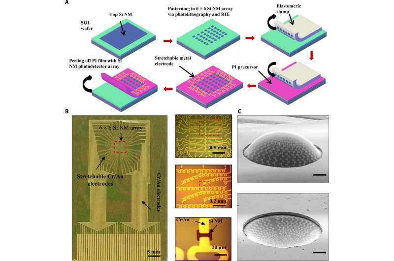
Fabrication of 6 × 6 Si NM array devices for strain-controlled stretchable PD. (A) Schematic illustration of device fabrication. RIE, reactive ion etching. (B) Photograph of a fabricated device on PI-coated SiO2/Si substrate and corresponding magnified view of device sections. (C) SEM images of convex (top) and concave (bottom) hemispherical shape of bulged PI film containing a 6 × 6 Si-NM PD array. Scale bars, 0.5 mm. Credit: Science Advances, doi: 10.1126/sciadv.abb0576
Silicon is widely used in the microelectronics industry although its photonics applications are restricted to the visible and partial near-infrared spectral range due to its fundamental optical bandgap. Researchers have therefore used recent advances in strain engineering to tailor material properties, including the optical bandgap. In a recent study now published on Science Advances, Ajit K. Katiyar and a group of scientists in electronic engineering and materials science in the Republic of Korea, reported strain-induced shrinkage in the silicon (Si) bandgap. The process facilitated photosensing beyond the fundamental limit within silicon nanomembrane photodetectors (abbreviated Si-NM PD). The team mechanically stretched the Si-NM PD pixels using a maximum strain of 3.5% to enhance photoresponsivity and extended the silicon absorption limit up to 1550 nm with applications suited for lidar sensors and obstacle detection during self-driving. They then developed a deformable three-dimensional (3-D) optoelectronics framework with concave and convex hemispherical architectures for electronic prototypes displaying wide-angle light detection, bioinspired by the biological eyes of insects.
Optoelectronic devices
Low-cost flexible and bendable optoelectronic devices including bioinspired imaging systems, photodetectors and photovoltaic cells can function under near-infrared (NIR) wavelength at room temperature. Photodetectors that can detect the short-wavelength infrared (SWIR) spectral range from 1300 to 2000 nm are in high demand for lidar sensors and for use in self-driving vehicles. Lidar devices provide an autonomous view of 360 degrees of surrounding objects to work as an eye of the driverless vehicle. Since the high-power light of ultraviolet-NIR wavelength can damage the retina of the human eye, SWIR light is fundamental to the lidar system. Theoretical claims suggest that the band structure of silicon can be substantially modified under the influence of compressive or tensile strain; therefore, materials scientists have used silicon as a basic building block in a variety of photonic applications. For instance, a reduced optical bandgap can capture photons with energies less than the fundamental gap of silicon for increased carrier mobility. Katiyar et al. therefore applied biaxial tensile strain onto the Si lattice and reported their photoresponse to be well beyond the optical bandgap limit of the material.
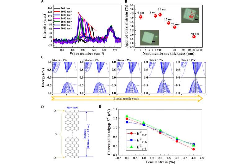
Strain and photodetection characteristics of single MSM device fabricated on 20 μm by 20 μm–sized 10-nm-thick Si NM and theoretical calculation of electronic band structure. (A) Raman spectra of 10-nm-thick Si NM sample recorded with increasing pressure. The spectra show the Raman scattering intensity enhancement and peak position shift toward the lower wave number side with increasing pressure. a.u., arbitrary units. (B) Maximum applied biaxial strain value in Si NMs of different thicknesses via the bulging process just before fracture. The inset shows the Si NM before (bottom left) and after fracture (top right). (C) Strain-dependent electronic band structure of 10-nm-thick Si NM with an applied biaxial strain of up to 4%. (D) Schematic representation of atomic arrangements of ~10-nm-thick Si NM used in theoretical calculation. (E) Bandgap values of different transitions extracted from the calculated energy band diagram for 10-nm-thick Si NM sample subjected to increasing biaxial tensile strain. Credit: Science Advances, doi: 10.1126/sciadv.abb0576
To demonstrate the SWIR imaging capability, the team fabricated metal-semiconductor-metal (MSM) type photodetector arrays on ultrathin silicon nanomembranes on a thin polymer substrate. The setup helped them realize imaging technologies such as lidar sensors and bioinspired imaging systems. The scientists patterned the target photodiode array matrix using photolithography and transferred the constructs onto a polyimide (PI) film and increased the pressure inside the sample holder cavity for the PI film to bulge and form convex and concave geometries while maintaining the fabricated arrays. They then measured the maximum strain value in the silicon nanomembrane samples of different thicknesses using Raman spectroscopy. Katiyar et al. calculated the electric energy band diagrams of 10-nm-thick silicon nanomembrane samples at different applied biaxial strain values ranging from 0 to 4% to understand the role of the bandgap reduction in SWIR light detection.
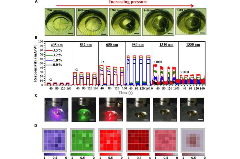
Strain-induced photoresponse and imaging characteristics of fabricated PD array. (A) Photograph of the 6 × 6 Si-NM PD array device mounted on bulge test setup with increasing pressure (scale bars, 1 mm). Photo credit: Ajit K. Katiyar, Yonsei University. (B) Strain-dependent transient photoresponse of single 10-nm-thick Si NM device measured under incident light of different wavelengths, from 405 to 1550 nm. The plots reveal the photosensing capability of the 10-nm-thick Si NM device beyond the Si photoabsorption wavelength range (400 to 1100 nm) under the applied strain. A clear on/off in photoresponse can be noticed under the 1550-nm light above the 3.5% applied biaxial strain. (C) Digital photographs of the Si-NM PD array device captured during imaging with lights of various wavelengths (scale bars, 3 mm). Photo credit: Ajit K. Katiyar, Yonsei University. (D) Corresponding photocurrent mapping images recorded under incident light of different wavelengths. Credit: Science Advances, doi: 10.1126/sciadv.abb0576
The working principle of the silicon nanomembrane photodetector (Si-NM PD)
The scientists examined strain-induced photosensing tunability with a single metal-semiconductor-metal-(MSM)-type photodetector engineered using a 10-nm-thick silicon nanomembrane. They calculated the photoresponsivity for each wavelength under increasing strain. The results led to the assumption that the increased photoresponsivity resulted from combined effects of enhanced optical absorption and photoinduced charge carrier mobilities at elevated strains. In theory the strain can substantially influence mobilities of charge carriers, the MSM devices therefore showed photosensing capabilities beyond the fundamental photoabsorption limit of silicon (approximating 1100 nm), with increased application of biaxial strain.
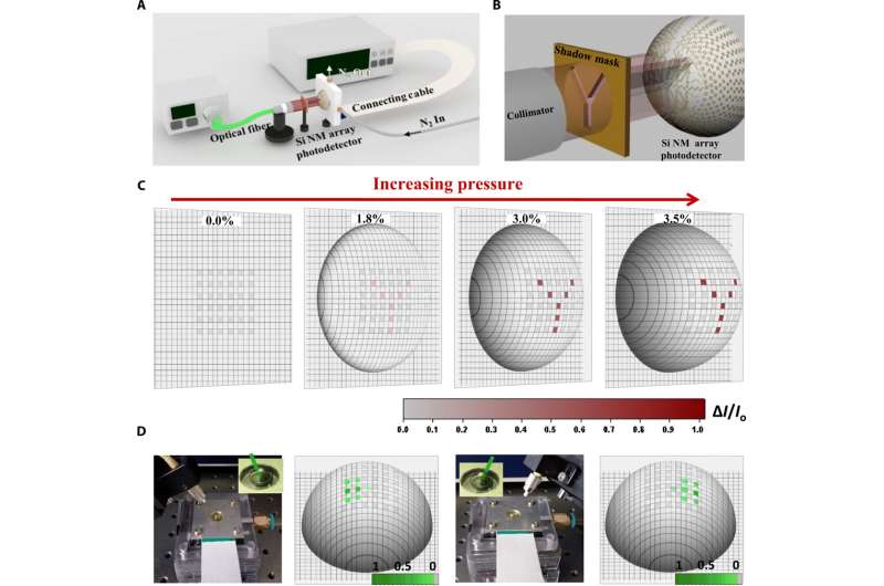
Overview of optical imaging system and object images obtained from 6 × 6 Si-NM PD array under increasing strain. (A) Schematic illustration of the overall imaging system and optical setup used for imaging of the letter Y containing a collimated light source, shadow mask, and device array. (B) Enlarged view of the schematic representation for imaging of Y alphabet. (C) Photocurrent mapping images of a representative letter recorded under incident light of 1310 nm with increasing straining pressure. An increase in photocurrent with increase in applied pressure is evident, which is a consequence of the increased strain in each Si NM pixel. (D) Photographic images and corresponding acquired mapping images of the fabricated PD pixel arrays under convex hemispherical geometry. The laser is projected at an incident angle of ~20° from the normal at both sides of the PD arrays. Photo credit: Ajit K. Katiyar, Yonsei University. Credit: Science Advances, doi: 10.1126/sciadv.abb0576
Katiyar et al. then monitored the strain-induced tunability of photodetection of silicon in the SWIR wavelength range under increasing strains. To accomplish this, they altered the lattice spacing of the silicon crystal by applying strain to modify or reduce its band structure for optical absorption in the SWIR region. After confirming SWIR photosensing features of a representative single silicon MSM device, they expanded their strain-induced SWIR imaging to a 6 x 6 Si-NM PD array prototype of convex and concave architectures.
Demonstrating strain-induced tuning and bioinspired convex and concave architectures
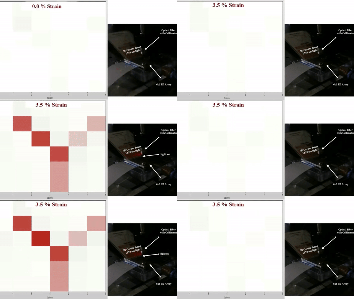
To demonstrate strain-induced tuning and its effect on photosensing, Katiyar et al. recorded a photocurrent pattern of the alphabet letter 'Y', which was first fabricated on a glass substrate in the form of a shadow mask. After reaching an approximate strain level of 1.8%, they recorded a noticeable photocurrent to clearly image 'Y' under a 1310-nm SWIR light. As the strain pressure in the bulge test cavity increased, the strain in each photodiode pixel also increased, eventually increasing the progression of the photocurrent to realize an image at a maximum strain of 3.5%. Using the pressure-induced bulging approach, the team achieved a convex hemispherical structure of the Si-NM PD pixel arrays that were also bioinspired by compound eyes of insects for wide-angle light detection.
Movie clip shows real time imaging of the “Y” shape with 1310 nm light projected onto a Si NM PD array system subjected to different strain levels. Left panel shows the real-time photocurrent map in a normalized color-coded scale generated using the output data collected from each PD pixel via the DAQ unit. Right panel shows the measurement system consisting of a PD array device mounted on bulge test setup, a fiber guided 1310 nm laser light and an IR card to visualize the incident laser pulse. It can be clearly noticed that there is no photoresponse from the PD pixels when they are at zero strain level. As the light is exposed onto the PD array subjected to a maximum biaxial strain of ~3.5%, a clear on-off representing “Y” shape can be realized. Photo credit: Ajit K. Katiyar, Yonsei University. Credit: Science Advances, doi: 10.1126/sciadv.abb0576
The team similarly engineered photodiode (PD) pixel arrays in reverse to produce a concave structure. The concave arrangement of PD pixels with inverted hemispherical geometry mimicked the concave focal plane of a mammalian eye. Using the concave setup, the team similarly conducted strain-driven imaging of the letter 'Y' under 1310-nm light exposure and different straining pressures. The team next recorded the photocurrent pattern of the letter 'I' with the photodiode matrix array under planar and concave architectures to understand the advantage of the concave surface on imaging, and noted the concave lens to provide a uniform and clearer representation of the letter 'I'.
In this way, Ajit K. Katiyar and colleagues demonstrated the improved photoresponse and SWIR (short-wavelength infrared) photosensing capabilities of silicon after subjecting the material to biaxial tensile strains. They created a platform using thin silicon nanomembranes mechanically stretched on a bulge setup to introduce strains. They reduced the optical bandgap of silicon by applying biaxial strain to detect incident photons beyond the fundamental optical absorption limit of the material. The team demonstrated the imaging capability using a 6 x 6 matrix metal-semiconductor-metal photodiode array with SWIR light. The researchers then constructed geometries that mimicked biological eyes using the hemispherical convex and concave shapes. The work allowed SWIR sensing in silicon via strain engineering with promising applications across silicon-based image sensors and photovoltaics.
More information: Ajit K. Katiyar et al. Breaking the absorption limit of Si toward SWIR wavelength range via strain engineering, Science Advances (2020). DOI: 10.1126/sciadv.abb0576
Young Min Song et al. Digital cameras with designs inspired by the arthropod eye, Nature (2013). DOI: 10.1038/nature12083
Rongrui He et al. Giant piezoresistance effect in silicon nanowires, Nature Nanotechnology (2006). DOI: 10.1038/nnano.2006.53
Journal information: Science Advances , Nature , Nature Nanotechnology
© 2020 Science X Network
