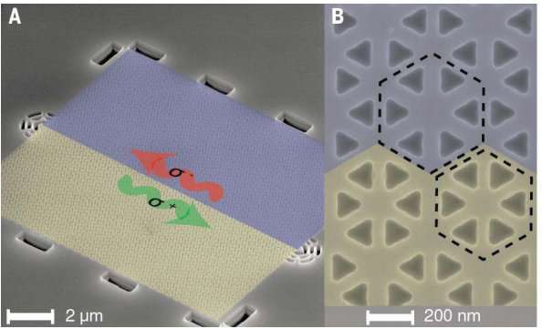
Fabricated device and band structure. (A) Scanning electron microscope image of the device, which is composed of two regions identified by blue and yellow shading, corresponding to two photonic crystals with different topological properties. The interface between the two photonic crystals supports helical edge states with opposite circular polarization (s+ and s– ). Grating couplers at each end of the device scatter light in the out-of-plane direction for collection. (B) Close-up image of the interface. Black dashed lines identify a single unit cell of each photonic crystal. Credit: Science 09 Feb 2018: Vol. 359, Issue 6376, pp. 666-668, DOI: 10.1126/science.aaq0327
A team of researchers at the University of Maryland has found a new way to route photons at the micrometer scale without scattering by building a topological quantum optics interface. In their paper published in the journal Science, the group describes their topological photonic structure, how it works, and the ways they tested it. Alberto Amo with Université de Lill in Spain offers a short history of recent attempts to route photons at such a tiny scale and also outlines the work done by the team at UM.
As Amo notes, scientists would like to be able to route photons with precision at the micrometer scale to create better integrated quantum optical circuits —a tendency of photons to scatter when meeting with bends and splitters has inhibited progress. In this new effort, the researchers have gotten around this problem by taking a new approach—using a semiconductor slab with triangular holes arranged in hexagon patterns. The slab was fashioned into a lattice of hexagons, with larger triangular holes on one side of the slab than the other. The routing occurred where the two types of hexagons met.
The architecture of the slab created edge states where two photonic crystals met—the bands touched and crossed over, producing edge states with energy between two crystal band gaps, allowing a photon to move between them without scattering. The arrangement of the hexagons provided band gaps next to one another from one side of the slab to the other, creating a channel of sorts for the photons to travel. Photons were provided courtesy of quantum dots that were embedded at border sites—firing a laser at the quantum dots caused them to generate individual photons, which then propagated along channels with no scattering. Photons that were of opposite polarization propagated in opposite directions.
The key to successfully building the structure was noting what happened when the quantum dots were excited with a high-powered laser—focusing the lens on just one side of an edge caused the emitted photon in the band gap to propagate without scattering. That led the team to fine-tune the size of the triangular holes and their distance from the center of their respective hexagons, allowing for the creation of the channels. The work, Amo suggests, is a big step toward the implementation of new kinds of optical circuits.
More information: A topological quantum optics interface, Science 09 Feb 2018: Vol. 359, Issue 6376, pp. 666-668, DOI: 10.1126/science.aaq0327
Abstract
The application of topology in optics has led to a new paradigm in developing photonic devices with robust properties against disorder. Although considerable progress on topological phenomena has been achieved in the classical domain, the realization of strong light-matter coupling in the quantum domain remains unexplored. We demonstrate a strong interface between single quantum emitters and topological photonic states. Our approach creates robust counterpropagating edge states at the boundary of two distinct topological photonic crystals. We demonstrate the chiral emission of a quantum emitter into these modes and establish their robustness against sharp bends. This approach may enable the development of quantum optics devices with built-in protection, with potential applications in quantum simulation and sensing.
Journal information: Science
© 2018 Phys.org


