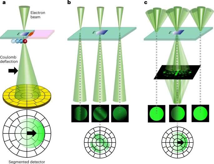
Schematic diagrams of the DPC STEM and tDPC STEM techniques. Credit: Nature Nanotechnology (2023). DOI: 10.1038/s41565-023-01349-8
The group led by Professor Naoya Shibata of the University of Tokyo, in collaboration with Sony Group Corporation, succeeded in directly observing a two-dimensional electron gas that accumulated at the semiconductor interface.
GaN-based devices are used as highly efficient light-emitting diodes (LEDs) and laser diodes (LDs). Because of their high dielectric breakdown strength and saturated electron velocity, these are expected to be used as next-generation high-frequency devices for communication and as power devices for power conversion.
In particular, high-electron-mobility transistors (HEMTs) generate a layer of accumulated electrons called a two-dimensional electron gas at the semiconductor interface. Electrons can move at high speeds in this layer, which makes the HEMTs excellent for high-frequency operation.
The details of this two-dimensional electron gas are crucial for the performance of semiconductor devices, and they have been estimated via indirect experiments or theoretical calculations. However, direct observation and confirmation of these phenomena are challenging.
In this study, the research group combined magnetic-field-free atomic resolution STEM (MARS) with an newly-developed tilt-scan system and ultrahigh-sensitivity, high-speed division-type detector to directly observe the two-dimensional electron gas that accumulated at the gallium nitride/aluminum indium nitride (GaN/AlInN) heterointerface.
The group conducted observations using the atomic resolution differential phase contrast (DPC) method, an atomic-level electromagnetic field observation technique developed by Professor Shibata and others. They successfully visualized and quantified the two-dimensional electron gas that accumulated in the several-nanometer-wide area of the semiconductor interface. These advances enabled control of the two-dimensional electron gas and are expected to further improve the performance of transistors.
The findings of this study have enabled the development of high-performance high-frequency/power devices that control two-dimensional electron gas, bringing about innovations in interface analysis and control of semiconductor devices. This has also led to groundbreaking measurement technologies that can significantly advance the research and development of cutting-edge materials and devices.
The research is published in the journal Nature Nanotechnology.
More information: Satoko Toyama et al, Real-space observation of a two-dimensional electron gas at semiconductor heterointerfaces, Nature Nanotechnology (2023). DOI: 10.1038/s41565-023-01349-8
Journal information: Nature Nanotechnology
Provided by Japan Science and Technology Agency


