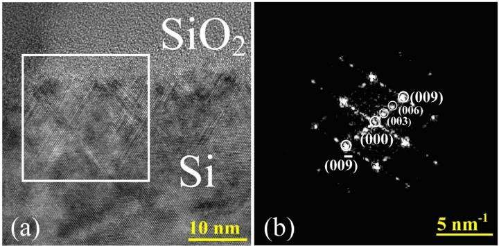
Electron microscopic image of the layer of the hexagonal silicon phase at the interface with the irradiated SiO2 film (a) and the pattern of diffraction reflexes obtained using the Fourier transform of the selected region (b). Credit: Lobachevsky University
A team of scientists from Lobachevsky University (Nizhny Novgorod, Russia) has obtained a material with a new structure for applications in next-generation optoelectronics and photonics. This material is one of the hexagonal modifications of silicon, which have better radiative properties compared to conventional cubic silicon, which is traditionally used in microelectronics.
The original technology for fabricating this material is based on implanting inert gas ions into a dielectric film on silicon in order to create mechanical stress. The relaxation of the stress during high-temperature annealing results in a phase transition in the silicon substrate at the interface with the dielectric layer. Thus, a near-surface layer with a new phase is formed in the initial silicon substrate. This layer can be used in optically active elements of integrated circuits.
According to one of the researchers, Alexey Mikhaylov, the problem of searching for light-emitting materials compatible with traditional silicon technologies has become particularly pressing during the last decade due to the need to further increase the speed of integrated circuits. At present, this speed is limited by the transmission rate of electrical signals inside the integrated circuit through metal conductors.
"One of the most promising approaches to overcoming this limitation is the use of optoelectronics when optical signals are used instead of electrical ones. Unfortunately, so far there are no technologies for creating silicon-based integrated circuits, in which data transfer will be carried out at the speed of light signals," says Alexey Mikhaylov.
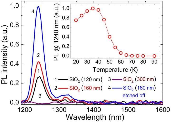
Photoluminescence spectra of samples with SiO2 films of various thickness, irradiated with Kr +, after annealing at 800°C. The inset shows the temperature dependence of the PL at the maximum for a sample with a film thickness of 160 nm. Credit: Lobachevsky University
Nizhny Novgorod scientists have synthesized silicon layers that can act as an optically active medium. Experimenters, engineers and theorists working in close interaction have studied in detail the synthesis conditions, optical properties and the electronic structure of these layers.
"Within the framework of this work, for the first time in the world, a hexagonal modification of silicon of the 9R phase was obtained by means of ion implantation, and an associated emission band was detected in the infrared region of the spectrum. This result is especially important, since this band is in the field of transparency of silicon light guides," Alexey Mikhaylov says.
Thus, the work of Nizhny Novgorod researchers can serve as a starting point for creating optoelectronic integrated circuits that will be manufactured using traditional technological operations and materials based on silicon.
More information: A. A. Nikolskaya et al, Light-emitting 9R-Si phase formed by Kr+ ion implantation into SiO2/Si substrate, Applied Physics Letters (2018). DOI: 10.1063/1.5052605
Journal information: Applied Physics Letters
Provided by Lobachevsky University


