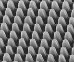
An nanoimprint mold made by Prof. Stephen Chou group at Princeton University
Nanoimprint is an emerging lithographic technology that promises high-throughput patterning of nanostructures. Based on the mechanical embossing principle, nanoimprint technique can achieve pattern resolutions beyond the limitations set by the light diffractions or beam scatterings in other conventional techniques. The article in the last issue of Journal of Physics D: Applied Physics by L. Jay Guo from The University of Michigan, reviews the basic principles of nanoimprint technology and some of the recent progress in this field.
Imprint lithography uses polymers that harden into patterns when exposed to ultraviolet light through a 1:1 proximity mask. The patterns on the template are written with an electron-beam system at the same line width as the pattern on the wafer, rather than at the 4x reduction possible with conventional optical lithography. Previously used only in making simple non-electronic structures such as optical gratings, the technique can make electronics by nanoimprinting multiple transistors with features two-thirds the size of those found on even the most advanced commercial chips. Even Intel is reportedly investigating the technology.
Nanoimprinting technique has enabled a parallel nanoscale processing capability with simple equipment. The simplicity of this method has made it appealing to researchers in various fields. Imprint lithography is relatively inexpensive because it avoids costly optics, as well as cumbersome enhancement techniques like phase-shift masks. The machines cost far less than today's step-and-scan systems.
Nano-imprint lithography is currently slated for the 32-nm node on the ITRS roadmap. The 32-nm node is expected to emerge in the 2009 time frame. Although no semiconductor firms make their commercial electronics using nanoimprinting, several have nanoimprinting tools in their research laboratories, and a number of firms sell the tools, including Molecular Imprints, EV Group, Obducat, and Nanonex.
If the defect density can be made low enough for volume production of large ICs and the current rate of progress on nanoimprint technology is maintained, this technique might even be able to challenge EUV.


