This article has been reviewed according to Science X's editorial process and policies. Editors have highlighted the following attributes while ensuring the content's credibility:
fact-checked
trusted source
proofread
Efficient heat dissipation perovskite lasers using a high-thermal-conductivity diamond substrate

Perovskite lasers have rapidly achieved progress in developing continuous-wave excited lasing from a femtosecond pulse excited lasing, which is considered a critical step towards electrically excited lasing. After continuous-wave lasing at room temperature, the next goal is to realize electrically driven lasing.
In commercially available electric injection lasers, traditional epitaxial grown single crystal semiconductors with both large thermal conductivity κ and high charge carrier mobility m usually exhibit small resistive heating under large current flow. While perovskites possess large and balanced charge carrier mobilities, they suffer from small κ values. The thermal conductivity of MAPbI3 is 1-3 W m−1 K−1, which is inferior to that of GaAs (50 W m−1 K−1).
Hence, heat converted from energy loss through nonradiative pathways cannot be effectively dissipated. This failure will increase the lasing threshold as carriers occupy a broader energy range at a higher temperature, diluting the population inversion of any given transition along with other problems such as degradation and heat-induced defects.
The lowest electric excitation threshold of a distributed-feedback (DFB) perovskite laser would be as high as 24 mA cm−2. Moreover, owing to high current injection in conventional perovskite light-emitting diode architectures used for laser devices, the external quantum efficiency would be significantly restricted under high current injection conditions owing to Joule heating. Hence, heat management is a bottleneck for developing perovskite-based electrically driven lasers.
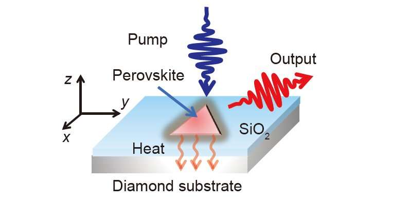
In this light, a group of researchers, including Prof. Guohui Li, Prof. Shengwang Yu, Prof. Yanxia Cui of Taiyuan University of Technology, and Prof. Kaibo Zheng of Lund University, demonstrated a perovskite nanoplatelet laser on a diamond substrate that can efficiently dissipate heat generated during optical pumping.
The demonstrated laser features a Q factor of ~1962, a lasing threshold of 52.19 μJ cm−2. Tight optical confinement is also realized by introducing a thin SiO2 gap layer between nanoplatelets and the diamond substrate. Electric field distributions inside the structures shows that a wide SiO2 gap of 200 nm in thickness produces evidently less leakage field in the diamond substrate, simultaneously proposing better mode confinement within the MAPbI3 nanoplatelet.
They evaluated the heat dissipation in perovskite nanoplatelet lasers on the diamond substrate by temperature variations under optical pumping conditions. The laser features a low pump-density-dependent temperature sensitivity (~0.56 ± 0.01 K cm2 μJ−1) through the incorporation of the diamond substrate.
The sensitivity is one to two orders of magnitude lower than the values for previously reported perovskite nanowire lasers on glass substrates. The high-thermal-conductivity diamond substrate enables the nanoplatelet laser to operate at a high pump density. The study could inspire the development of electrically driven perovskite lasers. This work was published in Science China Materials.
More information: Guohui Li et al, Efficient heat dissipation perovskite lasers using a high-thermal-conductivity diamond substrate, Science China Materials (2023). DOI: 10.1007/s40843-022-2355-6
Provided by Science China Press


