This article has been reviewed according to Science X's editorial process and policies. Editors have highlighted the following attributes while ensuring the content's credibility:
fact-checked
peer-reviewed publication
proofread
Controlled on-chip fabrication of large-scale perovskite single crystal arrays for laser and photodetector integration

Addressable active layers are highly required in optoelectronic devices to realize functional integration and application. Metal halide perovskites have shown promising applications in optoelectronic devices due to their superior optoelectronic properties and solution-based fabrication process.
However, due to the poor chemical stability of perovskite materials in polar solvents, the most commonly used photolithography and etching techniques for patterned single crystal arrays are highly incompatible with perovskite materials, which limits the development of perovskite in the field of optoelectronic devices. It is very important to find a preparation strategy of the perovskite single crystal array that can accurately control the properties of each pixel and align with optoelectronic device arrays.
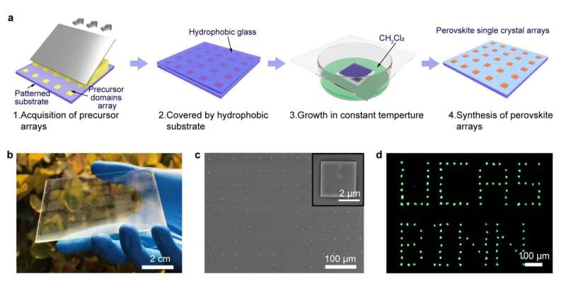
Recently, a new paper published in Light: Science & Applications, led by Professor Caofeng Pan from Beijing Institute of Nanoenergy and Nanosystems, Chinese Academy of Sciences and his cooperators reported an SC-ASC strategy of large-scale high-quality perovskite single crystal array for optoelectronic device integration.
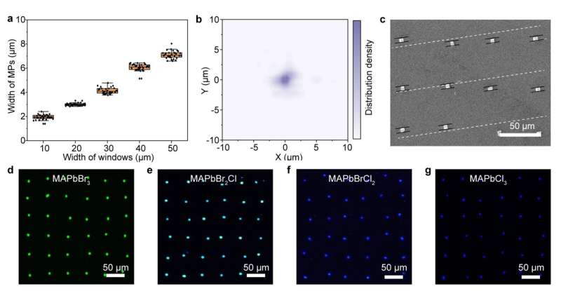
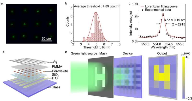
This method provides comprehensive control over the perovskite single crystal array, including the array shape and resolution with crystal dimension and position accuracy as well as the in-plane rotation of the individual single crystal in a large-scale array configuration. The as-fabricated perovskite single crystal can be served as a high-quality microcavity for WGM laser emission with a high Q factor of 2915 and a low threshold of 4.14 μJ/cm2.

Due to the readily regulation of the perovskite array as well as its excellent uniformity, a perovskite photodetector array based on the vertical structure has been demonstrated, showing a stable dynamic photobehavior and imaging capability. This approach for the fully controlled growth of perovskite array combining the conventional photolithography and solution processing procedures of perovskites offers a manufacturing platform for integrated functional photonics and optoelectronics.
The scientists summarize the keys to realizing fully controlled growth of high-quality perovskite arrays: "Substrate engineering defines the array resolution and pixel position, spatial confinement could regulate the extraction of contact lines to ensure that only one crystal is formed in the defined position, and antisolvent-assisted crystallization improves the crystal quality of each pixel."

"SC-ASC is an effective method for fabricating large-scale single-crystalline perovskite arrays because it incorporates the conventional photolithography process. 25 perovskite arrays have been demonstrated on a 10 × 10 cm glass substrate," they added.
"Since the readily regulation of the perovskite array as well as its excellent uniformity, the crystal arrays can be directly aligned for integration into large-scale optoelectronic devices. This landmark breakthrough in demonstrating fully controlled on-chip growth of the perovskite single crystal arrays could enable unprecedented applications in vision sensing, light imaging, and large-scale integrated devices," they predict.
More information: Zhangsheng Xu et al, Controlled on-chip fabrication of large-scale perovskite single crystal arrays for high-performance laser and photodetector integration, Light: Science & Applications (2023). DOI: 10.1038/s41377-023-01107-4
Journal information: Light: Science & Applications
Provided by Light Publishing Center, Changchun Institute of Optics, Fine Mechanics And Physics, CAS


