April 3, 2019 feature
Atomic switches by plasmonic heating of metallic contact points

Scientists have recently developed a light controlled nano-switch to lay groundwork for atomic device development in nanotechnology. They engineered the switches at the nanoscale in a first step toward fully integrated electronic device miniaturization. The multidisciplinary research was conducted by Weiqiang Zhang and co-workers, and an international team of collaborators. Results of the study are now published in Light: Science & Applications.
In the method developed by Zhang et al. light can be used to control electrical conductance at the junction between gold nano-electrodes by heating electrons at the electrode surface, in a technique known as 'plasmonic heating.' They validated the experimental mechanisms using simulations. The research team expanded electrodes via plasmonic heating to close the gap and turn the switch on, paving the way to build single-molecule transistors and nanopore-based biosensors at the nanoscale.
Molecular junctions were previously investigated as an approach to build nanoswitches by employing photochromic (light sensitive) molecules that switched between two distinct isoforms. The present work by Zhang et al. contrastingly demonstrated conductance switch behavior only with a bare metallic contact, under light illumination, without any molecules. They demonstrated the conductance of bare metallic quantum contacts as reversible switches across eight orders of magnitude to substantially exceed the performance of the previous molecular switches. The scientists were able to adjust the gap size between the two electrodes after the switch process with sub-angstrom accuracy, by controlling the light intensity or polarization.
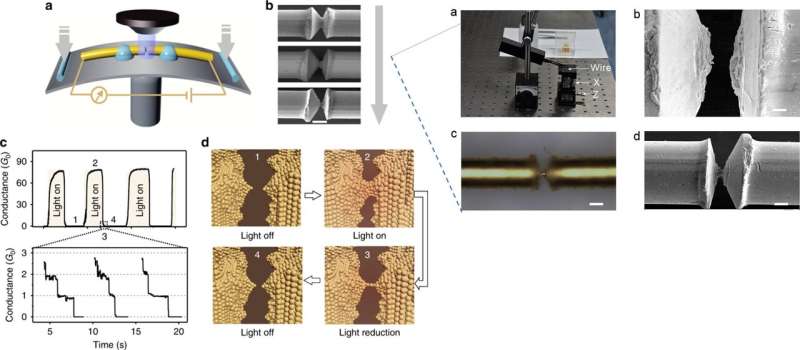
Engineering electronic devices using functional building blocks at the atomic scale is a major driving force in nanotechnology to form key elements in electronic circuits, which were previously miniaturized using mechanical tunneling, bias voltage/current operation and electrochemistry. Previous studies did not, however, address the concept of atomic switches controlled by plasmonic heating. Surface plasmons are coherent delocalized electron oscillations at the interface between two materials that form metallic nanostructures, which can be concentrated into the subwavelength gaps between the materials. In principle, when the resonance frequency of surface plasmons match the frequency of the incident light, the plasmon resonance is excited to produce strong light absorption and substantial plasmonic heating.
In the present study, Zhang et al. used this principle to show how a metallic, atomic scale contact could be operated reliably as a conductance switch through controlled illumination of light. To engineer the metallic atomic-scale contact they precisely stretched a metal nanowire using the mechanically controllable break junction. When they reduced the cross-section of the metal wire to a few nanometers or a few atoms, the diameter became comparable to the Fermi wavelength of the electrons, allowing quantum-mechanical effects to strongly influence the properties of electron transport. Using these principles, Zhang et al. showed how the conductance of an atomic gold contact could be switched from a few quanta of conductance to hundreds of quanta, and vice versa with light illumination. The scientists were able to reversibly switch the metallic quantum contacts between the open and closed state by controlling the light intensity. They created a nanogap between the quantum contacts within which coherent tunneling governed electron transport.
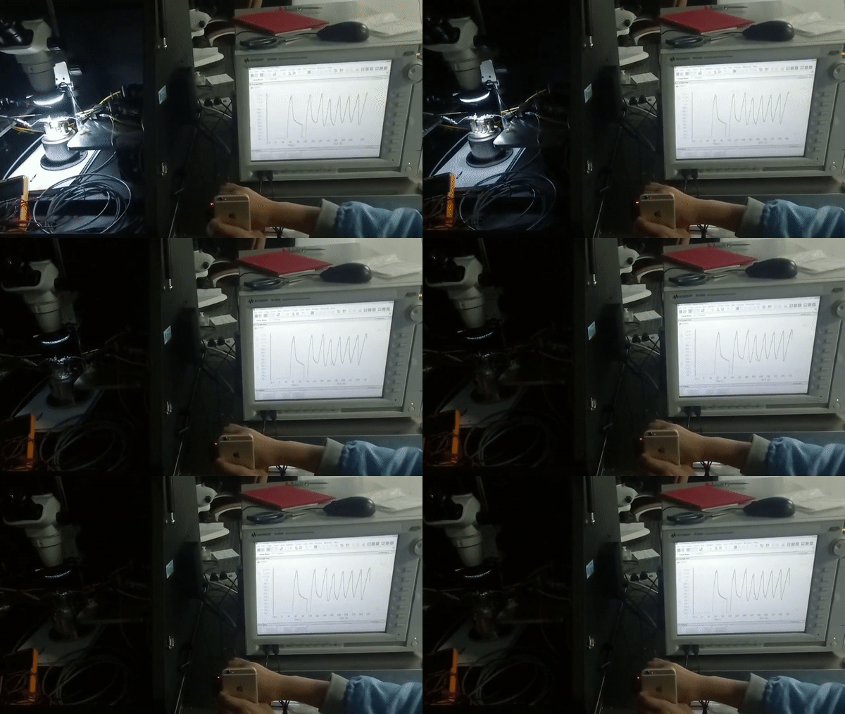
While generating a nanogap was crucial to fabricate single molecule-based devices, engineering an adjustable atomic-scale gap has remained a significant challenge. Although fixed gap sizes could not be adjusted post-fabrication, the gap-size could be readily and continuously adjusted through plasmonic heating at sub-angstrom resolution, as shown by Zhang and the research team.
For this, they used a commercial light-emitting diode (LED) lamp as a light source in the experiments with an AC adaptor to continuously control the intensity of light. The experimental setup did not require special optical hardware or high power laser sources. They used a commercially available gold wire with a constriction in the middle on a spring steel substrate to construct the nano contacts. Then using a 'mechanically controllable break junction' (MCBJ), the scientists stretched the constriction by bending the substrate, and observed it with scanning electron microscopy (SEM) images. Thereafter, the scientists reduced the cross-section of the constriction to form two separate electrodes. When they turned the light on, the conductance increased and decreased when the light was turned off; the large conductance resulting from light illumination strongly reconnected the two separated electrodes.
The scientists analyzed the phenomenon at the level of atomic arrangement, upon light illumination. They showed that the nanogaps had strong absorption of light in the visible and near infrared regions due to localized surface plasmon resonances (LSPR). When the frequency of the LED light matched the oscillation frequency of the free electrons and the electromagnetic field at the tip of the electrodes, the LSPR around the gap was excited. The absorbed light then converted to thermal energy causing nanoelectrode expansion and their reconnection. The conductance reached its maximum value when the system was at thermal equilibrium. When the light was shut off, the electrons separated once more.
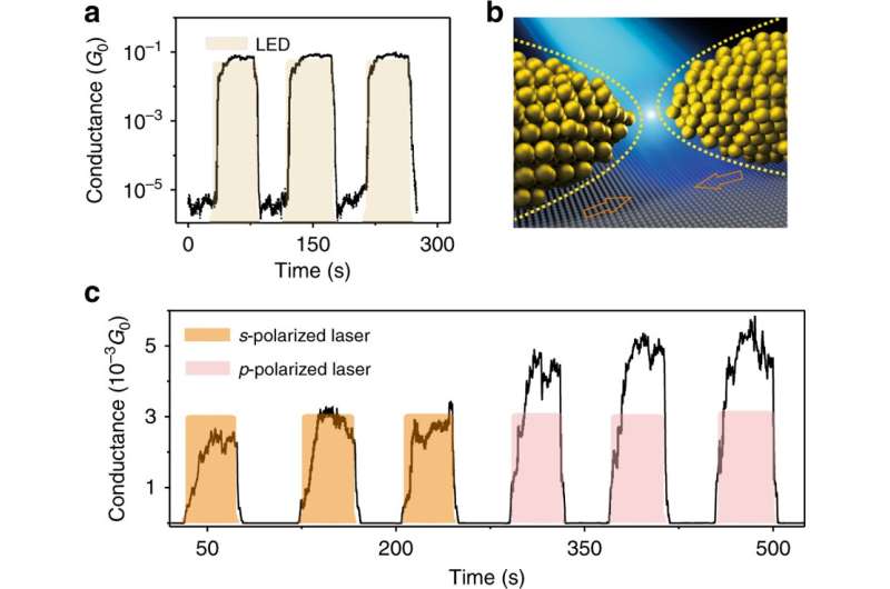
To understand how conductance depended on the light intensity, the scientists performed experiments where the maximum light intensity within each illuminated circle gradually increased. Zhang et al. showed that the maximum conductance in each circle increased approximately linearly with the intensity of light. They obtained repeatable data of the current as a function of the light intensity and showed how the conductance of quantum contact, could be regulated by the intensity of light.
Zhang et al. also observed how the nanogap size could be precisely modulated by light by showing that the conductance could be modified in the tunneling region, between the gap of the two electrodes, by controlling the LED light. When the light intensity was fixed, they could keep the tunneling current constant for longer. The scientists estimated the distance between the two electrodes using the Simmons equation; used to describe the relationship between the tunneling current and the tunneling gap size. They could thereby precisely control the distance between the two separated electrodes at sub-angstrom accuracy using the light intensity.
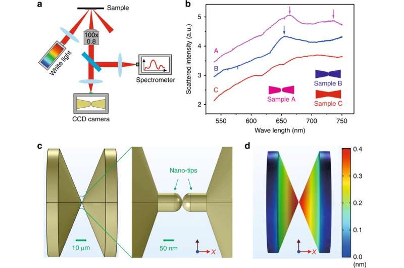
To confirm that the origin of switching behavior was plasmon-induced heating in the nanoscale plasmonic systems, the scientists investigated the scattering spectrum of the MCBJ samples to reveal the frequency of plasmonic resonance. The results indicated that the conductance change related to the expansion of the electrodes due to plasmonic heating. Zhang et al. also performed finite element method simulations to estimate the expansion of the electrodes and solved the electric field distribution, temperature distribution and thermal expansion on light illumination, using the COMSOL Multiphysics program package. The simulation calculated the maximum displacement of the electrodes as approximating 0.4 nm. Zhang et al. were able to further optimize the switching frequency by optimizing the characteristic dimensions for heat transfer. In this way, the scientists experimentally proved that atomic switches could be rapidly operated via plasmonic heating.
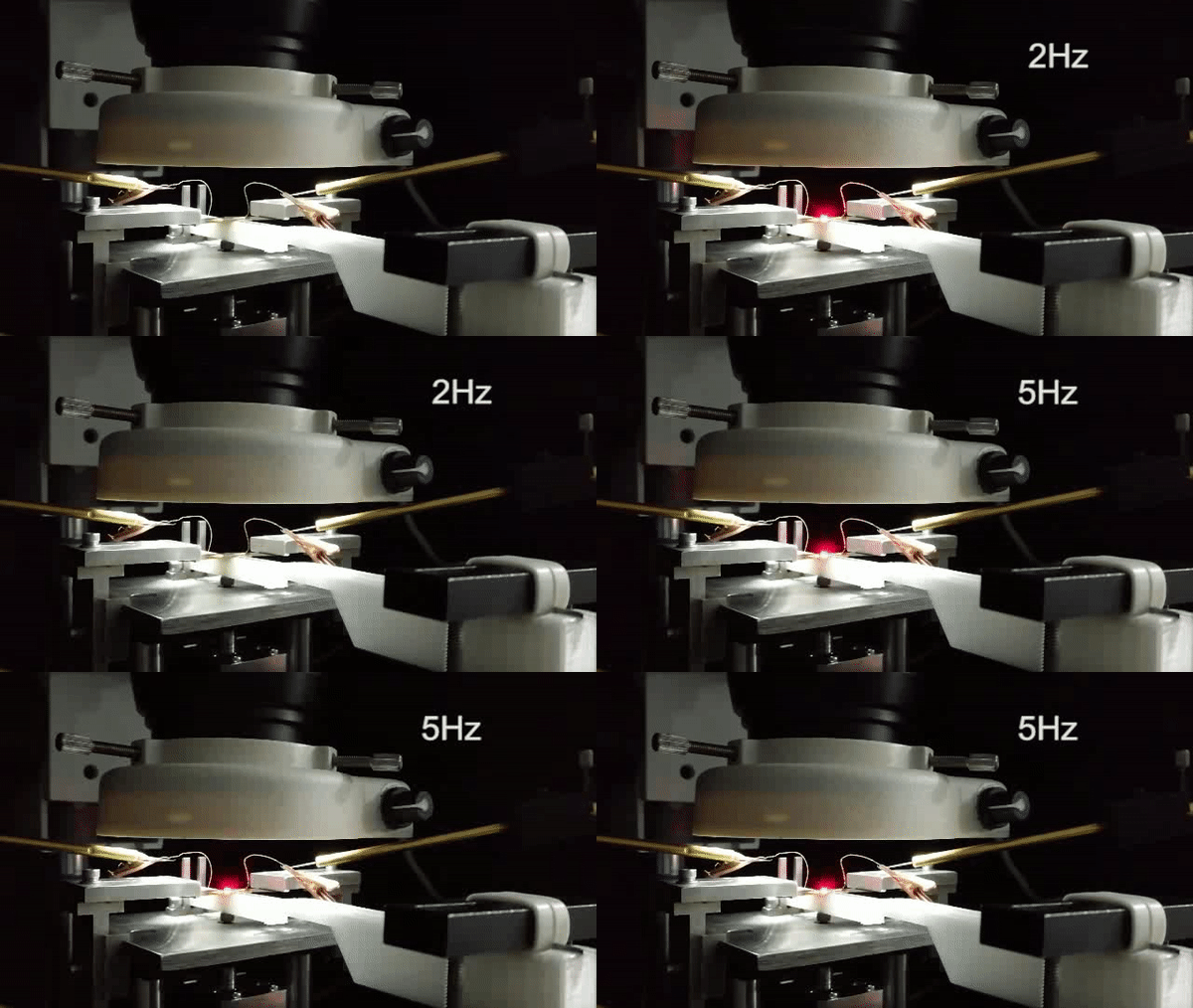
The work demonstrated the atomic geometry of metallic quantum contacts that could be modulated with light and the ability to reverse switch (on/off, vice versa) their conductance using plasmonic heating. While the atom-by-atom separation of electrodes were clearly observed, they could also adjust the gap size, between the electrodes at sub-angstrom resolution by controlling the intensity of light. Zhang et al. showed that the plasmon can potentially breakthrough the diffraction limit of light to realize nanofocusing, to transfer the plasmon-controlled atomic switch to realize highly integrated nanodevices; opening a new path to engineer nanoelectronic devices.
More information: Weiqiang Zhang et al. Atomic switches of metallic point contacts by plasmonic heating, Light: Science & Applications (2019). DOI: 10.1038/s41377-019-0144-z K.
Terabe et al. Quantized conductance atomic switch, Nature (2005). DOI: 10.1038/nature03190
Kasper Moth-Poulsen et al. Molecular electronics with single molecules in solid-state devices, Nature Nanotechnology (2009). DOI: 10.1038/nnano.2009.176
Tsuyoshi Hasegawa et al. Atomic Switch: Atom/Ion Movement Controlled Devices for Beyond Von-Neumann Computers, Advanced Materials (2011). DOI: 10.1002/adma.201102597
Journal information: Nature , Light: Science & Applications , Nature Nanotechnology , Advanced Materials
© 2019 Science X Network


