A chip-scale microscope for high-throughput fluorescence imaging

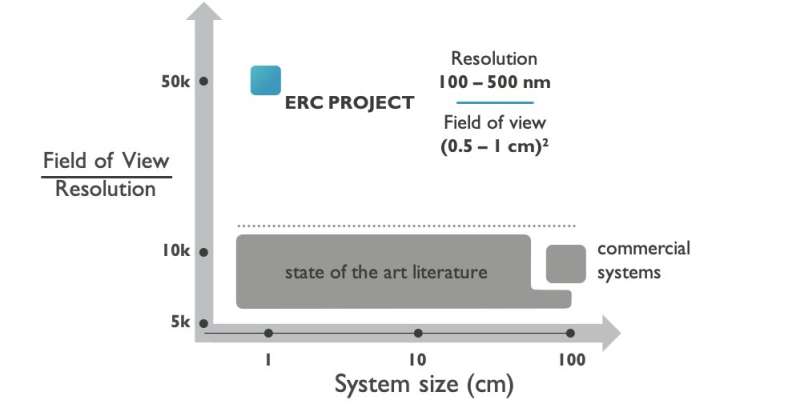
Conventional light microscopy has been instrumental for studying cells and microorganisms; fluorescence microscopy enabled visualization of even smaller cell features by selectively adding fluorescent labels to molecules. These microscopes are often comprise bulky and expensive systems that require regular maintenance to keep the lenses aligned. Additionally, they need to strike a compromise between device size, the size of the field of view, and resolution. For scientists to see more detail, larger optical components are required, but this causes the field of view to decrease.
Chip technology presents a whole different view on microscopy. Chips are compact and can integrate multiple functionalities. The scaling possibilities could allow chip-based microscopes to be produced at a fraction of the cost of standard devices. Niels Verellen, principal scientist at imec, has designed a high-resolution, on-chip microscope with a scalable field of view. At the halfway point of the five-year project, he talks about the early successes and challenges ahead.
Lens-free fluorescence microscopy
To downsize the microscope, Niels Verellen's team removed the quintessential part of standard optical microscopes: the lens. Lens-free options exist for light microscopy, which directly image scattered light. Imec's lens-free microscope, for example, uses the interference pattern of the excitation light to reconstruct the image holographically. These solutions don't work for fluorescence microscopy because fluorescence light is not coherent, meaning that there is no time-distance relationship between the excitation light and the fluorescence emission.
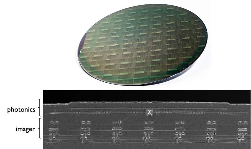
Niels Verellen says, "The goal of the ERC project is to achieve the same advantages as the existing lens-free optical microscope (small size, scalability, large field of view and high resolution) for fluorescence microscopy. The operating principle of our microscope is similar to that of a traditional confocal laser scanning fluorescence microscope. The lens-free microscope contains an image sensor (a pixel array), topped with an integrated photonic circuit consisting of waveguides and phase modulators that form focused illumination spots. Unlike in a confocal microscope that operates traditionally with one focus point, we can generate and scan many spots simultaneously."
"No lenses are needed: the integrated photonics circuit mimics all functions that the objective lens traditionally fulfills in a confocal microscope. The lens focuses laser light into a tiny spot to selectively excite the fluorophore in the sample. In our case, tiny light spots are generated in the integrated photonic circuit. The same lens in a confocal microscope collects the fluorescent light. If you use an objective lens with a higher numerical aperture, you can collect more light. Because the integrated photonic circuit where the spots are generated is very close to the image sensor, the numerical aperture of our microscope is inherently high."

High-throughput microscopy for next-gen sequencing
The chip presents a high-throughput alternative to conventional microscopy, especially for sequencing-related applications. Niels Verellen says, "We can only measure at the surface of a sample, within the evanescent field of total internally reflected light in a waveguide approximately 100nm deep). Aside from imaging membrane proteins, we see DNA sequencing as the most relevant application for our concept. DNA-tagging and optical detection form the backbone of next-generation sequencing, where the whole genome of an organism can be analyzed in one experiment. To sequence a genome, millions to trillions of fluorescently labeled nucleotides (A, G, T, C, the building blocks of DNA) need to be read out in a short time and at a reasonable cost. The on-chip microscope can scan the arrays of nucleotides at the surface and with high throughput. The scalability of the chips allows for massive parallelization of the experiments."
"That's one of the major advantages over confocal microscopy," explains Niels Verellen. "A confocal microscope costs over €100,000 and can scan a well plate with a limited number of DNA fragments or other molecules. Imec's microscope on-chip achieves the same resolution, but you can place ten chips side by side on a table at a fraction of the cost and floor space, and there is no need for expensive alignment maintenance. It removes the bottleneck of throughput."
Generating light spot patterns
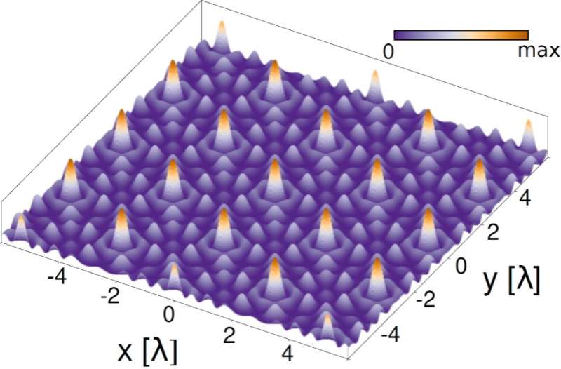
"The biggest challenge of this project is to create the high-resolution structured illumination pattern. In other words: how to generate the optimal pattern of light spots over a large field of view within the confines of a two-dimensional chip." The essential components in the photonic chip are waveguides that guide the light in the chip and phase modulators that shape the light for the sample illumination. Interference patterns can be generated using wave characteristics of the laser light. So a spot of light appears in regions where the combined waves reinforce each other (constructive interference) while it remains dark in regions where the waves cancel each other out (destructive interference). "To generate the desired pattern, precise control over the interfering waves is crucial. We successfully built a mathematical model that achieves the pattern with a limited number of components on the photonic chip. The model is based on prime number factorization to design a coherent optical lattice of light spots," explains Niels Verellen.

Optimization of the optical components
One of the main innovations was translating this theoretical model into a chip architecture that allows imaging. For that, the team had to optimize, redesign and de-risk all optical components in the circuit. The initial results on test chips (without imagers) showed that the interference patterns could be nicely controlled and modulated.
Additionally, the team had to develop a custom filter to place between the imager and the photonic circuit. This filter rejects the excitation light so that only the fluorescence emission reaches the imager. A standard fluorescence microscope uses interference filters that selectively reject a narrow range of wavelengths to achieve this. For it to work optimally, the objective lens needs to ensure that the fluorescent light hits the filter straight. "In the absence of a lens to take up the task of bundling the light, we can't use a standard interference filter," explains Niels Verellen. "Therefore, we developed a custom filter that covers a larger angular range."
"Until now, the components were designed and tested separately. However, we're expecting the first photonic circuits on the imagers out of the cleanroom," tells Niels Verellen. "The chips would be the first proof of concept device that can demonstrate the whole imaging concept. In parallel, we're already looking at ways to scale up to larger fields of view in the order of 1cm2," says Niels Verellen. "For that goal, we are working on several custom passive and active optical circuit components to shape and modulate the light in an efficient and fast way."

More information: Dmitry Kouznetsov et al, Revival and Expansion of the Theory of Coherent Lattices, Physical Review Letters (2020). DOI: 10.1103/PhysRevLett.125.184101
Journal information: Physical Review Letters
Provided by IMEC


