Building a better semiconductor

Research led by Michigan State University could someday lead to the development of new and improved semiconductors.
In a paper published in the journal Science Advances, the scientists detailed how they developed a method to change the electronic properties of materials in a way that will more easily allow an electrical current to pass through.
The electrical properties of semiconductors depend on the nature of trace impurities, known as dopants, which when added appropriately to the material will allow for the designing of more efficient solid-state electronics.
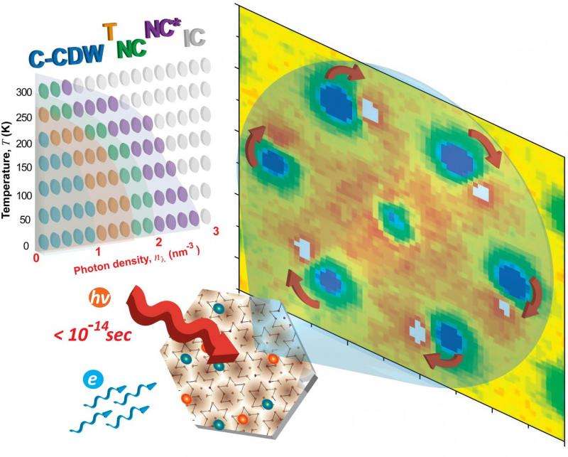
The MSU researchers found that by shooting an ultrafast laser pulse into the material, its properties would change as if it had been chemically "doped." This process is known as "photodoping."
"The material we studied is an unconventional semiconductor made of alternating atomically thin layers of metals and insulators," said Chong-Yu Ruan, an associate professor of physics and astronomy who led the research effort at MSU. "This combination allows many unusual properties, including highly resistive and also superconducting behaviors to emerge, especially when 'doped.'"
An ultrafast electron-based imaging technique developed by Ruan and his team at MSU allowed the group to observe the changes in the materials. By varying the wavelengths and intensities of the laser pulses, the researchers were able to observe phases with different properties that are captured on the femtosecond timescale. A femtosecond is 1 quadrillionth, or 1 millionth of 1 billionth, of a second.

"The laser pulses act like dopants that temporarily weaken the glue that binds charges and ions together in the materials at a speed that is ultrafast and allow new electronic phases to spontaneously form to engineer new properties," Ruan said. "Capturing these processes in the act allows us to understand the physical nature of transformations at the most fundamental level."
Philip Duxbury, a team member and chairperson of the department of physics and astronomy, said ultrafast photo-doping "has potential applications that could lead to the development of next-generation electronic materials and possibly optically controlled switching devices employing undoped semiconductor materials."
A semiconductor is a substance that conducts electricity under some conditions but not others, making it a good medium for the control of electrical current. They are used in any number of electronics, including computers.
More information: Exploration of metastability and hidden phases in correlated electron crystals visualized by femtosecond optical doping and electron crystallography, advances.sciencemag.org/content/1/5/e1400173
Journal information: Science Advances
Provided by Michigan State University


