Researchers create sub-10-nanometer graphene nanoribbon patterns

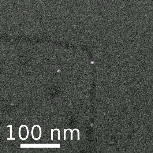
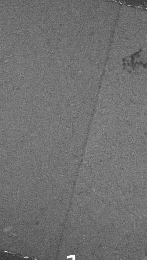
New research at Rice University shows how water makes it practical to form long graphene nanoribbons less than 10 nanometers wide.
And it's unlikely that many of the other labs currently trying to harness the potential of graphene, a single-atom sheet of carbon, for microelectronics would have come up with the technique the Rice researchers found while they were looking for something else.
The discovery by lead author Vera Abramova and co-author Alexander Slesarev, both graduate students in the lab of Rice chemist James Tour, appears online this month in the American Chemical Society journal ACS Nano.
A bit of water adsorbed from the atmosphere was found to act as a mask in a process that begins with the creation of patterns via lithography and ends with very long, very thin graphene nanoribbons. The ribbons form wherever water gathers at the wedge between the raised pattern and the graphene surface.
The water formation is called a meniscus; it is created when the surface tension of a liquid causes it to curve. In the Rice process, the meniscus mask protects a tiny ribbon of graphene from being etched away when the pattern is removed.

Tour said any method to form long wires only a few nanometers wide should catch the interest of microelectronics manufacturers as they approach the limits of their ability to miniaturize circuitry. "They can never take advantage of the smallest nanoscale devices if they can't address them with a nanoscale wire," he said. "Right now, manufacturers can make small features, or make big features and put them where they want them. But to have both has been difficult. To be able to pattern a line this thin right where you want it is a big deal because it permits you to take advantage of the smallness in size of nanoscale devices."
Tour said water's tendency to adhere to surfaces is often annoying, but in this case it's essential to the process. "There are big machines that are used in electronics research that are often heated to hundreds of degrees under ultrahigh vacuum to drive off all the water that adheres to the inside surfaces," he said. "Otherwise there's always going to be a layer of water. In our experiments, water accumulates at the edge of the structure and protects the graphene from the reactive ion etching (RIE). So in our case, that residual water is the key to success.
"Nobody's ever thought of this before, and it's nothing we thought of," Tour said. "This was fortuitous."
Abramova and Slesarev had set out to fabricate nanoribbons by inverting a method developed by another Rice lab to make narrow gaps in materials. The original method utilized the ability of some metals to form a native oxide layer that expands and shields material just on the edge of the metal mask. The new method worked, but not as expected.
"We first suspected there was some kind of shadowing," Abramova said. But other metals that didn't expand as much, if at all, showed no difference, nor did varying the depth of the pattern. "I was basically looking for anything that would change something."
It took two years to develop and test the meniscus theory, during which the researchers also confirmed its potential to create sub-10-nanometer wires from other kinds of materials, including platinum. They also constructed field-effect transistors to check the electronic properties of graphene nanoribbons.
To be sure that water does indeed account for the ribbons, they tried eliminating its effect by first drying the patterns by heating them under vacuum, and then by displacing the water with acetone to eliminate the meniscus. In both cases, no graphene nanoribbons were created.
The researchers are working to better control the nanoribbons' width, and they hope to refine the nanoribbons' edges, which help dictate their electronic properties.
"With this study, we figured out you don't need expensive tools to get these narrow features," Tour said. "You can use the standard tools a fab line already has to make features that are smaller than 10 nanometers."
Provided by Rice University


