Caltech engineers invent light-focusing device

(Phys.org)—As technology advances, it tends to shrink. From cell phones to laptops—powered by increasingly faster and tinier processors—everything is getting thinner and sleeker. And now light beams are getting smaller, too.
Engineers at the California Institute of Technology (Caltech) have created a device that can focus light into a point just a few nanometers (billionths of a meter) across—an achievement they say may lead to next-generation applications in computing, communications, and imaging.
Because light can carry greater amounts of data more efficiently than electrical signals traveling through copper wires, today's technology is increasingly based on optics. The world is already connected by thousands of miles of optical-fiber cables that deliver email, images, and the latest video gone viral to your laptop.
As we all produce and consume more data, computers and communication networks must be able to handle the deluge of information. Focusing light into tinier spaces can squeeze more data through optical fibers and increase bandwidth. Moreover, by being able to control light at such small scales, optical devices can also be made more compact, requiring less energy to power them.
But focusing light to such minute scales is inherently difficult. Once you reach sizes smaller than the wavelength of light—a few hundred nanometers in the case of visible light—you reach what's called the diffraction limit, and it's physically impossible to focus the light any further.
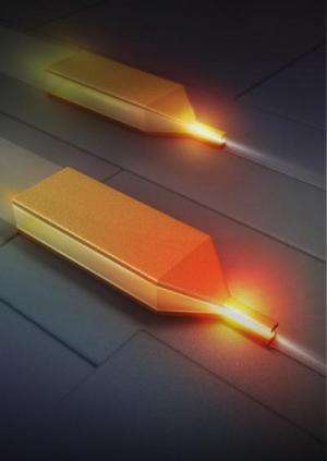
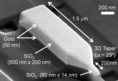
But now the Caltech researchers, co-led by assistant professor of electrical engineering Hyuck Choo, have built a new kind of waveguide—a tunnellike device that channels light—that gets around this natural limit. The waveguide, which is described in a recent issue of the journal Nature Photonics, is made of amorphous silicon dioxide—which is similar to common glass—and is covered in a thin layer of gold. Just under two microns long, the device is a rectangular box that tapers to a point at one end.
As light is sent through the waveguide, the photons interact with electrons at the interface between the gold and the silicon dioxide. Those electrons oscillate, and the oscillations propagate along the device as waves—similarly to how vibrations of air molecules travel as sound waves. Because the electron oscillations are directly coupled with the light, they carry the same information and properties—and they therefore serve as a proxy for the light.

Instead of focusing the light alone—which is impossible due to the diffraction limit—the new device focuses these coupled electron oscillations, called surface plasmon polaritons (SPPs). The SPPs travel through the waveguide and are focused as they go through the pointy end.
Because the new device is built on a semiconductor chip with standard nanofabrication techniques, says Choo, the co-lead and the co-corresponding author of the paper, it is easy integrate with today's technology
Previous on-chip nanofocusing devices were only able to focus light into a narrow line. They also were inefficient, typically focusing only a few percent of the incident photons, with the majority absorbed and scattered as they traveled through the devices.
With the new device, light can ultimately be focused in three dimensions, producing a point a few nanometers across, and using half of the light that's sent through, Choo says. (Focusing the light into a slightly bigger spot, 14 by 80 nanometers in size, boosts the efficiency to 70 percent). The key feature behind the device's focusing ability and efficiency, he says, is its unique design and shape.
"Our new device is based on fundamental research, but we hope it's a good building block for many potentially revolutionary engineering applications," says Myung-Ki Kim, a postdoctoral scholar and the other lead author of the paper.
For example, one application is to turn this nanofocusing device into an efficient, high-resolution biological-imaging instrument, Kim says. A biologist can dye specific molecules in a cell with fluorescent proteins that glow when struck by light. Using the new device, a scientist can focus light into the cell, causing the fluorescent proteins to shine. Because the device concentrates light into such a small point, it can create a high-resolution map of those dyed molecules. Light can also travel in the reverse direction through the nanofocuser: by collecting light through the narrow point, the device turns into a high-resolution microscope.
The device can also lead to computer hard drives that hold more memory via heat-assisted magnetic recording. Normal hard drives consist of rows of tiny magnets whose north and south poles lay end to end. Data is recorded by applying a magnetic field to switch the polarity of the magnets.
Smaller magnets would allow more memory to be squeezed into a disc of a given size. But the polarities of smaller magnets made of current materials are unstable at room temperature, causing the magnetic poles to spontaneously flip—and for data to be lost. Instead, more stable materials can be used—but those require heat to record data. The heat makes the magnets more susceptible to polarity reversals. Therefore, to write data, a laser is needed to heat the individual magnets, allowing a surrounding magnetic field to flip their polarities.
Today's technology, however, can't focus a laser into a beam that is narrow enough to individually heat such tiny magnets. Indeed, current lasers can only concentrate a beam to an area 300 nanometers wide, which would heat the target magnet as well as adjacent ones—possibly spoiling other recorded data.
Because the new device can focus light down to such small scales, it can heat smaller magnets individually, making it possible for hard drives to pack more magnets and therefore more memory. With current technology, discs can't hold more than 1 terabyte (1,000 gigabytes) per square inch. A nanofocusing device, Choo says, can bump that to 50 terabytes per square inch.
Then there's the myriad of data-transfer and communication applications, the researchers say. As computing becomes increasingly reliant on optics, devices that concentrate and control data-carrying light at the nanoscale will be essential—and ubiquitous, says Choo, who is a member of the Kavli Nanoscience Institute at Caltech. "Don't be surprised if you see a similar kind of device inside a computer you may someday buy."
The next step is to optimize the design and to begin building imaging instruments and sensors, Choo says. The device is versatile enough that relatively simple modifications could allow it to be used for imaging, computing, or communication.
Journal information: Nature Photonics
Provided by California Institute of Technology


