This article has been reviewed according to Science X's editorial process and policies. Editors have highlighted the following attributes while ensuring the content's credibility:
fact-checked
proofread
Laser manufacturing of spatial resolution approaching quantum limit
. DOI: 10.1038/s41377-023-01354-5")
Since early demonstrations of femtosecond laser as a three-dimensional (3D) processing tool, microdevices with exciting optical, electronic, mechanical, and magnetic functions have been manufactured, by which novel concepts from 3D quantum photonic integrated circuits to intelligent micro-robots are enabled.
Much effort in the past decade in this field has been devoted to improving manufacture spatial resolution, and several tens of nanometer feature sizes have been reported based on multiphoton absorption, stimulation emission depletion, far-field-induced near-field enhancement, and photoexcitation-induced chemical bonding effects. Nevertheless, advanced applications, such as single-electron transistors, single-photon emitters (SPE), single-atom memory, or quantum-bit devices, require higher manufacturing spatial resolution (less than 10 nm, far beyond the optical diffraction limit).
In a new paper published in Light Science & Application, a team of scientists, led by Professor Hongbo Sun from State Key Laboratory of Precision Measurement Technology and Instruments, Department of Precision Instrument, Tsinghua University, Beijing, China, and co-workers have proposed and experimentally demonstrated close-to-atom scale manufacturing using a threshold tracking and lock-in (TTL) method, by which feature sizes of
Through this approach, researchers could achieve near unity yield fabrication of single photon sources with high positional accuracy and minimal damage to the lattice. These single photon sources exhibit high brightness, high emission purity, and high stability.
This close-to-atom scale laser manufacturing represents a significant step forward in scalable quantum photonic technologies. The scientists summarize the principle of TTL technology:
"The idea is to use the additional laser pulses (probe light) to precisely track whether atomic or close-atomic scale damage occurs under the initial pulse (fabricating light). The intrinsic damage threshold of the target material is precisely locked. It is worth mentioning that this feedback method does not depend on the detection sensitivity of the instrument, and can accurately lock the intrinsic damage threshold of the target material for nanoscale laser manufacturing."
-
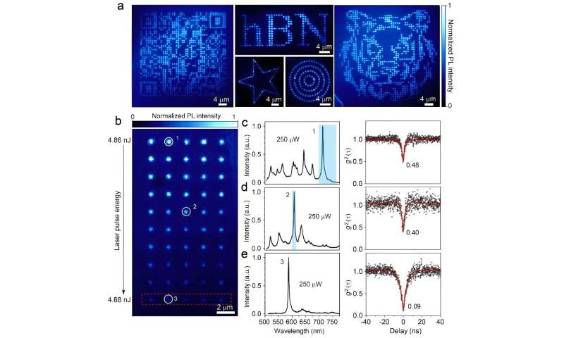
Deterministic creation of single-photon colour centres. Credit: Light: Science & Applications (2024). DOI: 10.1038/s41377-023-01354-5 -
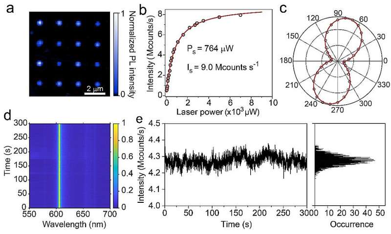
High reproducibility, high brightness, and high durability of single-photon single colour centres. Credit: Light: Science & Applications (2024). DOI: 10.1038/s41377-023-01354-5
"We demonstrated that the laser manufacturing accuracy in this work has reached the quantum limit, which is a new milestone after the optical diffraction limit. When the laser energy approaches the near-atomic scale damage threshold, the laser ablation of individual atoms does not necessarily occur in the geometric center of the focused spot."
"This is because, in this limit state, the gradient provided by the laser energy (the top of the Gaussian distribution) will be very flat. The breakdown region defined by the laser energy gradient will fail, and local atomic ablation will randomly occur in a certain region (~ a few nanometers, the specific value is related to the target material), which will be dominated by the position and energy fluctuations of local electrons, rather than the power density slope of the incident laser."
"By TTL technology, the near unity yield manufacturing of single photon sources with nanoscale positioning precision could be realized. Meanwhile, these single photon sources exhibit excellent properties including high brightness (emitting nearly ten million photons per second), high emission purity, and high stability."
"This result suggests the high potential of close-to-atom scale laser manufacturing for the application of quantum devices."
More information: Xiao-Jie Wang et al, Laser manufacturing of spatial resolution approaching quantum limit, Light: Science & Applications (2024). DOI: 10.1038/s41377-023-01354-5
Provided by TranSpread


