This article has been reviewed according to Science X's editorial process and policies. Editors have highlighted the following attributes while ensuring the content's credibility:
fact-checked
peer-reviewed publication
trusted source
proofread
Study demonstrates atomic layer deposition route to scalable, electronic-grade van der Waals tellurium thin films

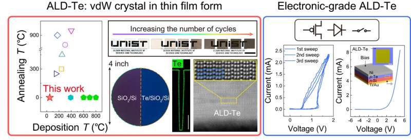
A research team, led by Professor Joonki Suh in the Department of Materials Science and Engineering and the Graduate School of Semiconductor Materials and Devices Engineering at UNIST, has made a significant breakthrough in thin film deposition technology. By employing an innovative atomic layer deposition (ALD) process, Professor Seo successfully achieved regular arrangement of tellurium (Te) atoms at low temperatures as low as 50 degrees Celsius.
The ALD method is a cutting-edge thin film process that enables precise stacking of semiconductor materials at the atomic layer level on three-dimensional structures—even at low process temperatures. However, traditional application to next-generation semiconductors requires high processing temperatures above 250 degrees Celsius and additional heat treatment exceeding 450 degrees Celsius.
In this research, the UNIST team applied ALD to monoelemental van der Waals tellurium—a material under extensive investigation for its potential applications in electronic devices and thermoelectric materials.
Remarkably, they successfully fabricated high-quality Te thin films without any post-deposition heat treatment at an unprecedentedly low temperature of only 50 degrees Celsius. The resulting films exhibited exceptional uniformity with precisely controlled thickness down to nanometers scale—achieving perfect atom arrangement with one out of every billion atoms.
To enhance reactivity at lower temperatures, the research team employed two precursors with acid-base properties. Additionally, they introduced co-reactants to improve surface reactions and stability while adopting a repeating dosing technique by injecting precursors in shorter intervals. These strategies enabled the production of dense and continuous Te thin films compared to conventional methods that often resulted in porous or discontinuous grain depositions.
The developed manufacturing process allowed for wafer-scale growth on entire 4-inch (100mm) wafers, providing precise atomic layer-level thickness control and uniform deposition. Furthermore, the Te thin films demonstrated compatibility with vertical three-dimensional structures—a crucial requirement for high device integration. This breakthrough holds significant potential for various electronic devices such as transistors, rectifiers, and selection elements.
"This research fulfills all the essential criteria of low-temperature, large-area, and high-quality synthesis in semiconductor deposition processes," stated Professor Suh.
The results of this research were published in ACS Nano.
More information: Changhwan Kim et al, Atomic Layer Deposition Route to Scalable, Electronic-Grade van der Waals Te Thin Films, ACS Nano (2023). DOI: 10.1021/acsnano.3c03559
Journal information: ACS Nano


