This article has been reviewed according to Science X's editorial process and policies. Editors have highlighted the following attributes while ensuring the content's credibility:
fact-checked
trusted source
proofread
Advancing 2D materials: Achieving the goal with UV-assisted atomic layer deposition

In 2004, the public first became acquainted with graphene- a remarkably thin, flexible, and electrically conductive material possessing considerable strength. However, harnessing graphene's potential as a component has presented numerous challenges.
For instance, creating electrode-based transistors requires depositing extremely thin dielectric films. Regrettably, this process has led to a reduction in graphene's electrical properties and caused defects during implementation.
A research team comprising of co-researchers including Professor Jihwan An from the Department of Mechanical Engineering at Pohang University of Science and Technology (POSTECH), Dr. Jeong Woo Shin from the Department of Mechanical Engineering at NTU Singapore, and Geonwoo Park from the Department of MSDE at SEOULTECH employed a novel approach called UV-assisted atomic layer deposition (UV-ALD) to treat graphene electrode.
This pioneering technique resulted in successful production of high-performance graphene-dielectric interface. Their findings were featured in Advanced Electronic Materials.
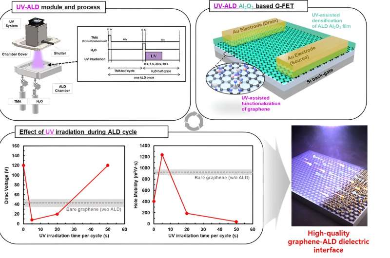
The research team became the first to apply UV-ALD to the deposition of dielectric films onto the surface of graphene which is a 2D material. Atomic layer deposition (ALD) involves adding ultra-thin layers at the atomic scale to a substrate, and its significance has grown considerably as semiconductor components have shrunk in size. UV-ALD, which combines ultraviolet light with the deposition process, enables more dielectric film placement than traditional ALD. However, no one had explored the application of UV-ALD for 2D materials such as graphene.
The research team employed UV light with a low energy range (below 10 eV) to deposit atomic layer dielectric films onto the graphene surface, effectively activating the graphene surface without compromising its inherent properties. This activation was achieved under specific conditions (within 5 seconds per cycle during the ALD process), demonstrating the possibility of depositing high-density, high-purity atomic layer dielectric films at low temperatures (below 100℃).
Furthermore, when graphene field effect transistors were fabricated using UV-ALD process, the graphene's exceptional electrical properties remained intact. The outcome was a three-fold increase in charge mobility and a significant reduction in Dirac voltage due to the reduced defects on the graphene surface.
Professor Jihwan An who led the research explained, "Through UV-ALD, we achieved high-performance graphene-dielectric interface." He further added, "Our study resulted in uniform atomic layer deposition without compromising the properties of this 2D material. I hope this development will pave the way for the next-generation semi-conductor and energy devices."
More information: Geonwoo Park et al, High‐Performance Graphene‐Dielectric Interface by UV‐Assisted Atomic Layer Deposition for Graphene Field Effect Transistor, Advanced Electronic Materials (2023). DOI: 10.1002/aelm.202300074
Provided by Pohang University of Science and Technology


