December 18, 2019 feature
A skin-like 2-D pixelized full-color quantum dot photodetector

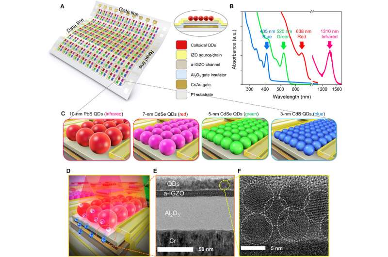
Full-color photodetectors that can convert light to electric signals without sophisticated color filters and interferometric optics have gained considerable attention for widespread applications. However, technical challenges have impeded scientists from combining multispectral semiconductors and improving photon-transfer efficiency to form high-performance optoelectronic devices in practice. In a recent report on Science Advances, Jaehyun Kim and a research team in materials science and engineering in the U.S. and Korea, described a low-temperature fabricated (150 degrees C), two-dimensionally (2-D) pixelated, full-color photodetector using monolithic integration of quantum dots coupled to amorphous indium-gallium-zinc-oxide semiconductors.
They introduced chelating chalcometallate (combined synthetic metal/semiconductor) ligands to successfully realize highly efficient charge carrier transport and photoresistor-free fine patterning of 2-D layers. The constituents showed extremely high photodetectivity and photoresponsivity across a broad range of wavelengths. Based on these techniques, the research team implemented a wavelength discriminable phototransistor circuit array on a skin-like soft platform as a versatile and scalable approach to form wide spectral image sensors and human-oriented biological devices.
Materials scientists aim to develop interconnected full-color [ranging across the ultraviolet (UV) spectrum to infrared (IR)] photodetectors engineered on a skin-like soft platform to collect meaningful information from the human body and the surrounding environment. Such technologies will have applications as neuromorphic image sensors, soft robotics and as biological health monitors. Compared to single- or narrow-band photodetection, 2-D full-color photodetection on a single platform is significantly advantageous to obtain reliable and extensive information. To overcome existing challenges of 2-D full-color device fabrication, researchers had previously developed photodetectors with new photosensing materials to form device architectures for broadband photodetection. These include colloidal quantum dots, amorphous oxide semiconductors (AOSs), organic semiconductors, perovskite materials and 2-D materials such as graphene and transition metal dichalcogenides.
While previous advances are noteworthy, they typically included a narrow-band absorbing material with limited bandgap tunability and limited wavelength discriminating ability. To overcome limits, colloidal quantum dots (QDs) have gained attention due to their unique optoelectronic characteristics including wide bandgap tunability and increased light absorption coefficients. But they remain rarely reported during applications of highly sensitive full-color photodetection.

In the new study, Kim et al. developed a versatile and large-area scalable approach to extend the detection bandwidth of a photodetector from UV to IR. The scientists used monolithic integration of QDs with amorphous indium-gallium-zinc-oxide (a-IGZO)-based thin-film transistors (TFTs) or phototransistors to implement a low-temperature 2-D in-pixel charge integrating circuit (CIC) array for color discrimination. To achieve ultrahigh photodetectivity, they introduced an electrically high-performing and trap-reduced chelating chalcometallate ligand (combined metallic and semiconductor ligand) for QDs (quantum dots). Kim et al. also obtained high-resolution patterning of multiple QD layers via direct photopatterning and demonstrated their pixelized phototransistors to form a skin-like, two-dimensional photodetector capable of position-dependent full-color photodetection.
The research team conducted two strategies to realize full-color photodetection with high sensitivity; first they designed the photodetector architecture alongside an in-pixel circuit for high sensitivity. They then combined QDs with an a-IGZO (indium-gallium-zinc-oxide) active layer for full color light absorption and highly efficient charge collection. They engineered the flexible QD/a-IGZO photodetector on an ultrathin polyimide (PI) substrate. Then used cross-sectional high-resolution transmission electron microscopy (HRTEM) to confirm stacking of QDs on the a-IGZO layer, alongside uniform distribution of the QD layer. To detect the full color range, the team included a variety of QD layers with different bandgaps on the a-IGZO layer.
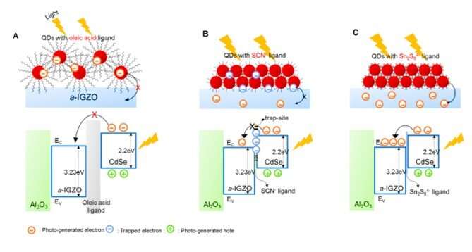
Scientists had previously embedded semiconducting QDs in several optoelectronic devices, but charge transport remained frequently limited by ligands connecting the QDs. To enhance charge transfer efficiency of the device, they investigated conducting ligands including ethanedithiol, thiocyanate and atomic ligands. The present team of researchers chose Sn2S64- as the ideal system from a variety of chalcometallate ligands and selected SCN- ligand-based QDs as a reference—due to wide investigations to their high-conductivity and mobility in electronic devices.

In the experimental setup, SCN- capped QDs easily decomposed to form sulfur vacancies on the QD surface, preventing efficient charge transfer between the QDs and the a-IGZO channel layer. Comparatively, the bidentate (donating two pairs of electrons to a metal atom) Sn2S64- ligands had minimal sulfur vacancies on the QD surface. The photogenerated electrons from Sn2S64- capped QDs therefore efficiently transferred into the conduction band of the a-IGZO channel layer. This resulted in a large energy barrier and charge collection with minimal trapping for the photogenerated holes to remain in the QDs or near the QD/a-IGZO interface.
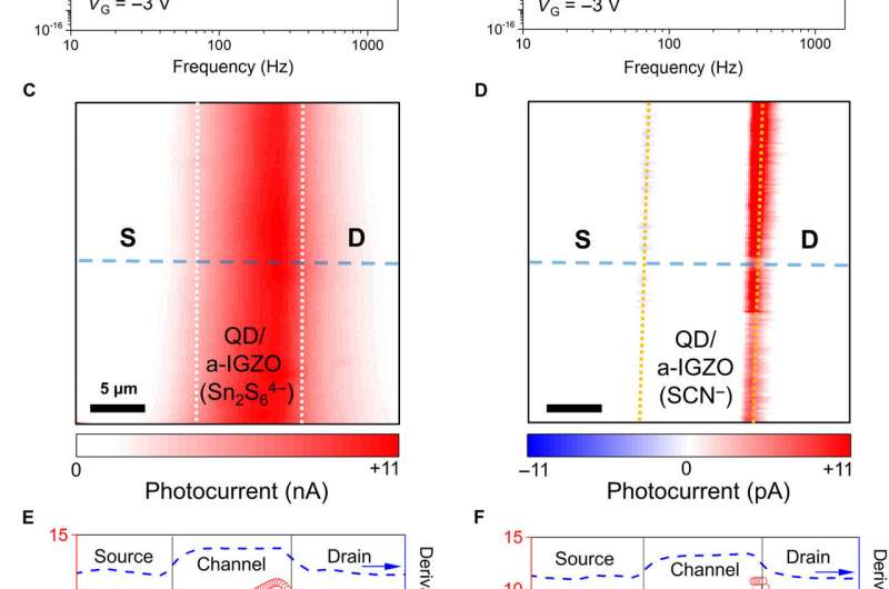
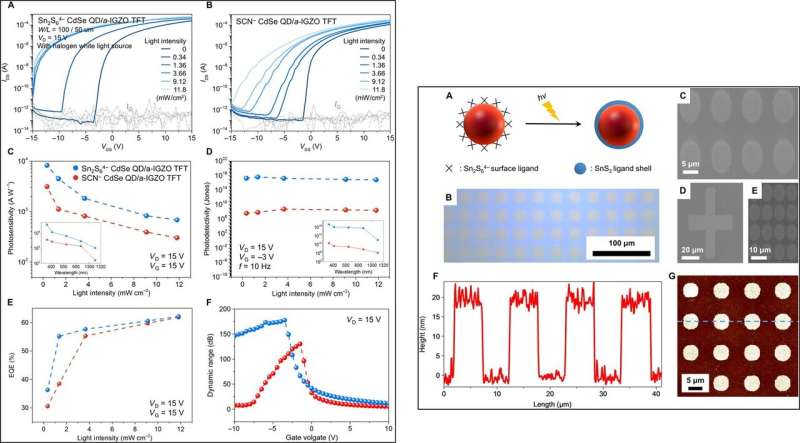
The scientists investigated optical response characteristics of QD/a-IGZO phototransistors with a variety of spectroscopic analyses, including interfacial trap-related noise analysis and scanning photocurrent microscopy (SPCM). They noted the SCN- capped cadmium selenide (CdSe) phototransistors to have approximately 103 times higher trap density than Sn2S64- capped CdSe QD/a-IGZO phototransistors. The Sn2S64- capped phototransistor exhibited a large Gaussian current profile with a photovoltaic-dominated process, whereas the SCN- capped phototransistor showed a clear photothermoelectric response. As a result, Kim et al. observed the photocurrent level of Sn2S64- capped devices to be much higher than SCN- capped devices, due to the efficient transfer of photogenerated electrons from CdSe QDs to the a-IGZO layer without a charge carrier trapping problem.

The research team compared the photosensitivity and photodetectivity of the two phototransistors under white light and broadband illumination to observe high photoresponse in Sn2S64- capped phototransistors. They credited the outcome to the extremely low flicker noise of the device and high conducting and trap-reduced Sn2S64- ligands of CdSe QDs. Kim et al. further recorded a smaller photoresponse from 0.27 seconds to 90 milliseconds; sufficient for photodetection and image-sensing applications.
To guarantee high photodetectivity and reduce current leaks in the devices, they patterned high-resolution QD layers using a CMOS-compatible, direct photopatterning process. Using field-enhanced scanning electron microscopy (FESEM) and atomic force microscopy (AFM) images, the researchers confirmed clear patterning of QD layers with a thickness approximating 17 nm. After engineering a full-color (UV-to-IR) charge integrating circuit (CIC) containing directly photopatterned QD layers, they used an a-IGZO layer as a channel material to control or switch and wavelength-discriminate the integrated circuits. The experimental setup allowed in-pixel amplification, full-color and UV detection.
![LEFT: CIC array characteristics for full-color discrimination. (A) Schematic diagram of CIC and logic table of full-color signal detection in one pixel. (B) Optical micrograph of the partially patterned QDs including IR PbS (T1, 10 nm), red CdSe (T2, 7 nm), green CdSe (T3, 5 nm), and blue CdS (T4, 3 nm) and bare a-IGZO phototransistors and the schematic of amplification circuit. RTN is the channel resistance of load TFTs (T1 to T4), and RT6 is the channel resistance of driver TFT (T6). Here, channel width/length are 100/50 μm (load TFTs), 200/10 μm (T5), and 5/200 μm (T6). Scale bar, 50 μm. (C to G) Photoresponse characteristics of T1, T2, T3, T4, and T5/T6 with respect to wavelength of light. (H) Output current of the five-channel full-color photodetector. (I) Mixed light discrimination. Light intensities of UV, blue, green, and red are 1 mW cm−2, while that for IR is 13.6 mW cm−2. For yellow, red (0.5 mW cm−2) and green (0.5 mW cm−2) were mixed, and for cyan, green (0.5 mW cm−2) and blue (0.5 mW cm−2) were mixed. Photo credit: Jaehyun Kim, Displays and Devices Research Lab. School of Electrical and Electronics Engineering, Chung-Ang University, Seoul 06974, Korea. RIGHT: Full-color two-dimensional mapping applications. (A) Schematic illustration of the 10 by 10 CIC array. (B) Optical micrograph of the 10 by 10 CIC array on an ultrathin PI substrate and the associated circuit schematic (right). Scale bars, 1 mm and 300 μm (inset). (C) Relevant intensity profile reconstructed from output current mapping of the 10 by 10 CIC array on an ultrathin PI substrate with respect to the wavelength of light [IR (1310 nm), R (638 nm), G (520 nm), B (406 nm), and UV (365 nm)]. Light intensities of UV, blue, green, and red are 1 mW cm−2, while that for IR is 13.6 mW cm−2. Scale bar, 3 mm. (D) Round and stripe shape two-dimensional mapping images with white light illumination (halogen lamp with 1.36 mW cm−2). Scale bar, 3 mm. (E) Photograph of band-type flexible health monitoring system composed of four light sources and phototransistor-based circuit arrays (CIC) attached onto an index fingertip. (F) Full-color two-dimensional biological mapping images of human fingertip with respect to the wavelength of light. Light intensities of blue, green, and red are 3 mW cm−2, while that for IR is 13.6 mW cm−2. Each light is placed on the subject’s finger, and the transmitted light is collected with the phototransistor-based CIC array placed below the finger. Photo credit: Jaehyun Kim, Displays and Devices Research Lab. School of Electrical and Electronics Engineering, Chung-Ang University, Seoul 06974, Korea. Credit: Science Advances, doi: 10.1126/sciadv.aax8801 A skin-like two-dimensionally pixelized full-color quantum dot photodetector](https://scx1.b-cdn.net/csz/news/800a/2019/4-askinliketwo.jpg)
To demonstrate possible applications of the skin-like full-color photodetector platform, Kim et al. prepared a 10 x 10 multiplexed QD/a-IGZO photodetector array on a PI (polyimide) substrate and acquired a large amount of wavelength-dependent data. The team 2-D mapped the output current obtained from the photodetector array under illumination of five different light sources (infrared, red, green, blue and UV), where most of the pixels showed spatially uniform current distribution to the corresponding sources of light. Kim et al. then used the device for biological applications and monitored blood oxygen saturation levels in the index finger by measuring various wavelengths of light through the capillary blood vessels. The resulting 2-D map data for diverse light sources showed specific transmittance depending on the wavelength. The results can lead to critical advancement of more reliable and precise diagnostics in health monitoring systems.
In this way, Jaehyun Kim and colleagues presented low-temperature fabricated, diverse QD-based phototransistors and their in-pixel CIC arrays to outperform conventional photodiode-based sensors. The devices resolved existing confines of state-of-art flexible photodetectors for full-color photodetection from UV to IR for highly reliable, 2-D photodetection. The wavelength discriminating potential of the device can open new prospects for photodetecting devices and electronics. Similarly, the photosensitive and high-conductive chelating chalcometallate ligands perfectly transferred photogenerated electrons to an active semiconductor layer, without electron trapping for extremely high photosensitivity and photodetection. The platforms can be embedded to engineer a facile route for a variety of bio-imaging applications.
More information: Jaehyun Kim et al. A skin-like two-dimensionally pixelized full-color quantum dot photodetector, Science Advances (2019). DOI: 10.1126/sciadv.aax8801
Stijn Goossens et al. Broadband image sensor array based on graphene–CMOS integration, Nature Photonics (2017). DOI: 10.1038/nphoton.2017.75
Michael A. Boles et al. The surface science of nanocrystals, Nature Materials (2016). DOI: 10.1038/nmat4526
Journal information: Science Advances , Nature Photonics , Nature Materials
© 2019 Science X Network


