New form of crystalline order holds promise for thermoelectric applications

Since the 1850's scientists have known that crystalline materials are organized into fourteen different basic lattice structures. However, a team of researchers from Vanderbilt University and Oak Ridge National Laboratory (ORNL) now reports that it has discovered an entirely new form of crystalline order that simultaneously exhibits both crystal and polycrystalline properties, which they describe as "interlaced crystals."
Writing in the Nov. 14 issue of the journal Nature Communications, the researchers describe finding this unusual arrangement of atoms while studying nanoparticles made from the semiconductor copper-indium sulfide (CIS), which is being actively studied for use in solar cells. The interlaced crystal arrangement has properties that make it ideal for thermoelectric applications that turn heat into electricity, they report. The discovery of materials with improved thermoelectric efficiency could increase the efficiency of electrical power generation, improve automobile mileage and reduce the cost of air conditioning.
"We discovered this new form while studying nanoparticles," said Sokrates Pantelides, University Distinguished Professor of Physics and Engineering at Vanderbilt, who coordinated the study. "It most likely exists in thin films or bulk samples, but it has apparently gone unnoticed."
In crystalline materials, atoms are arranged in periodic arrays of points, a mathematical abstraction called a Bravais lattice. There are 14 different types of Bravais lattices in three dimensions. The same atom or group of atoms sits at each lattice point. The simplest and most symmetric is the "simple cubic" lattice. Square floor tiles provide a two-dimensional example. The corners of the tiles create a regular, repeating lattice pattern. A three-dimensional version is the face centered cubic (FCC), which has points both on the corners and at the centers of the faces of a cube.
A number of minerals have an FCC lattice. Imagine shrinking an FCC lattice, down to the atomic scale and placing different atoms at each lattice point. When you have more than one atom at each point, each type of atom forms its own sub-lattice. For example, if you put a pair of carbon atoms at each point (forming two FCC sub-lattices), you get diamond. If you put a pair of sodium and chlorine atoms at each lattice point, they form sodium and chlorine sub-lattices and you get salt.
CIS is a bit more complicated. You can think of the sulfur atoms occupying one FCC sub-lattice while the copper and indium atoms share a second sub-lattice. Each copper or indium atom is surrounded by four nearest-neighbor sulfur atoms while each sulfur is surrounded by two copper and two indium nearest-neighbors.

Bulk CIS generally has a cubic structure. But, when Vanderbilt Assistant Professor of Chemistry Janet Macdonald and her post-doctoral student Emil Hernandez-Pagan grew nanocrystals of CIS to explore their properties for solar light harvesting, they found that the tiny crystals had a hexagonal lattice structure, with the sulfur atoms occupying one sub-lattice and the copper and indium atoms sharing another.
"In CIS, the sulfur atoms make these perfectly packed layers and the copper and Indium ions lie in between, like jam in a sandwich. Emil was making nanoparticles of this material in the lab, but we didn't know if the copper and indium were ordered or just randomly distributed in the 'jam' layers," said Macdonald. "This was important because disordered structures generally have poor electrical properties."
Because of the small size of nanoparticles, X-ray diffraction, the normal method for determining crystal structure, could not tell whether the copper and indium atoms were ordered in some fashion.
Vanderbilt Research Assistant Professor Xiao Shen in Pantelides' group performed theoretical calculations to determine whether an ordered or disordered distribution of the copper and indium atoms was preferred and concluded that several different ordered structures were preferred over a disordered structure and all the ordered structures had an equal likelihood of occurring.
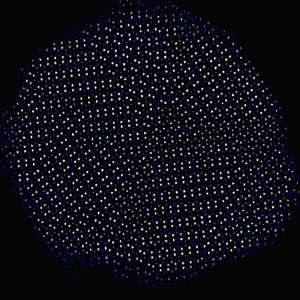
The scientists didn't have a clear idea about how these different ordered structures could coexist until Wigner Fellow Wu Zhou at ORNL successfully obtained detailed atomic-scale images of the nanoparticles. His images clearly showed that, while all atoms occupy the points of a perfect hexagonal Bravais lattice, the copper and indium atoms form a series of distinct domains where the copper and indium atoms are arranged differently. The boundaries between distinct copper-indium arrangements are similar to grain boundaries in polycrystalline solids, but both
Shen's calculations and the images revealed that the underlying hexagonal lattice is totally undisturbed.
When the researchers analyzed the images even more closely, "then things got even more interesting," Macdonald said. "We discovered it was really hard to decide exactly where the edges were between the areas of different ordering. Usually it is really clear because normally when you have polycrystalline samples, there is strain at the edges between the different areas. So it was very strange that there seemed to be no strain or breaks at the edges.
The underlying lattice was completely unperturbed by these different regions of copper/indium ordering. It was really quite amazing that despite all these little crystallites, the whole crystal lattice is completely happy and doesn't need to shift or twist or break to accommodate them."
According to the researchers, the interlaced crystal structure may be just what is needed to optimize thermoelectric applications for power generation or cooling. Thermoelectric devices need a material that is an excellent electrical conductor and a poor conductor of heat. The problem is that materials like metals that are good electrical conductors also tend to be good heat conductors and vice versa. Defects and grain boundaries that retard heat flow also reduce electrical conductivity.
"We haven't tested this yet, but we are confident that these materials have high electrical conductivity and low thermal conductivity...just what you need for thermoelectrics. The field is now wide open for scientists who can fabricate thin films and make thermoelectric measurements," said Pantelides.
Journal information: Nature Communications
Provided by Vanderbilt University


