Genetic approach helps design broadband metamaterial

A specially formed material that can provide custom broadband absorption in the infrared can be identified and manufactured using "genetic algorithms," according to Penn State engineers, who say these metamaterials can shield objects from view by infrared sensors, protect instruments and be manufactured to cover a variety of wavelengths.
"The metamaterial has a high absorption over broad bandwidth," said Jeremy A. Bossard, postdoctoral fellow in electrical engineering. "Other screens have been developed for a narrow bandwidth, but this is the first that can cover a super-octave bandwidth in the infrared spectrum."
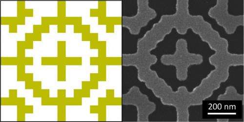
Having a broader bandwidth means that one material can protect against electromagnetic radiation over a wide range of wavelengths, making the material more useful. The researchers looked at silver, gold and palladium, but found that palladium provided better bandwidth coverage. This new metamaterial is actually made of layers on a silicon substrate or base. The first layer is palladium, followed by a polyimide layer. On top of this plastic layer is a palladium screen layer. The screen has elaborate, complicated cutouts—sub wavelength geometry—that serve to block the various wavelengths. A polyimide layer caps the whole absorber.
"As long as the properly designed pattern in the screen is much smaller than the wavelength, the material can work effectively as an absorber," said Lan Lin, graduate student in electrical engineering. "It can also absorb 90 percent of the infrared radiation that comes in at up to a 55 degree angle to the screen."

To design the necessary screen for this metamaterial, the researchers used a genetic algorithm. They described the screen pattern by a series of zeros and ones—a chromosome—and let the algorithm randomly select patterns to create an initial population of candidate designs. The algorithm then tested the patterns and eliminated all but the best. The best patterns were then randomly tweaked for the second generation. Again the algorithm discarded the worst and kept the best. After a number of generations the good patterns met and even exceeded the design goals. Along the way the best pattern from each generation was retained. They report their results in a recent issue of ACS Nano.
"We wouldn't be able to get an octave bandwidth coverage without the genetic algorithm," said Bossard. "In the past, researchers have tried to cover the bandwidth using multiple layers, but multiple layers were difficult to manufacture and register properly."
This evolved metamaterial can be easily manufactured because it is simply layers of metal or plastic that do not need complex alignment. The clear cap of polyimide serves to protect the screen, but also helps reduce any impedance mismatch that might occur when the wave moves from the air into the device.

"Genetic algorithms are used in electromagnetics, but we are at the forefront of using this method to design metamaterials," said Bossard.
Journal information: ACS Nano
Provided by Pennsylvania State University


