October 30, 2013 feature
Through a nanopore, ionically: Graphene quantum transistor for next-generation DNA sensing

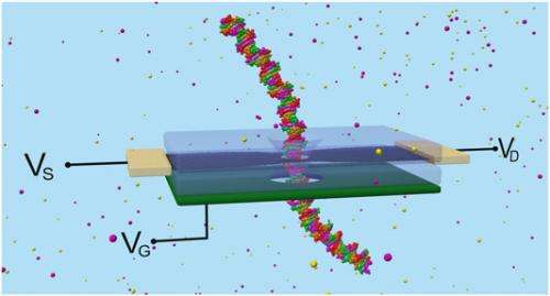
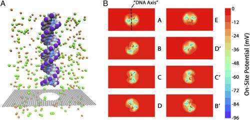
(Phys.org) —In the ongoing quest to devise faster, lower-cost methods for sequencing the human genome, scientists at University of Illinois at Urbana–Champaign have developed a novel approach: DNA molecules are sensed by passing them through a layer of constricted graphene embedded in a solid-state membrane containing a nanopore (a small hole with a roughly 1 nm internal diameter), located in a graphene nanoribbon (GNR). A critical feature of the new paradigm is that graphene's electrical properties allow the layer to be tuned in several distinct ways – namely, altering the shape of its edge, carrier concentration and nanopore location – thereby modulating both electrical conductance and external charge sensitivity. The researchers found that their novel technique can detect the DNA strand's rotational and positional conformation, and demonstrated that a graphene membrane with quantum point contact geometry exhibits greater electrical sensitivity than on with so-called uniform armchair geometry. The team has proposed a graphene-based field-effect transistor-like device for DNA sensing.
Prof. Jean-Pierre Leburton briefed Phys.org on the research he and his colleagues – Anuj Girdhar, Chaitanya Sathe and Klaus Schulten – conducted. "Simulations are presently leading experimental efforts on this specific topic – but transport models based on density functional theory cannot handle a large number of atoms due to limited computational resources," Leburton tells Phys.org, recounting some of the challenges the scientists faced. (Density functional theory, or DFT, is a quantum mechanical modeling method used in physics and chemistry to investigate the electronic structure of many-body systems.)
"In addition," Leburton continues, "these models are restricted to solid-state systems, while we're dealing with a hybrid solid-liquid system. For this reason, very simplistic and idealistic physical conditions are assumed on graphene nanoribbons." Such assumptions include uniform GNR widths with perfect armchair or zigzag edges, the nanopore being placed in the center of the graphene nanoribbon, and an absence of electrostatic perturbations from either the electrolytic solution or the dielectric supporting the graphene nanoribbon."In our approach, we use a multiorbital tight-binding (TB) technique that can handle a much larger number of atoms than DFT to account for the non-uniform GNR width, its irregular edges, and various sizes and positions of the nanopore," Leburton explains. (The TB technique uses a superposition of wave functions of isolated atoms located at each atomic site to calculate the electronic band structure of solids.)
"The electronic spectrum obtained from the tight binding model is then fed into a transport model based on a non-equilibrium Green function technique to compute the electrical conductance in general GNR configurations." A non-equilibrium Green (aka Green's) function, or NEGF, can be used to solve an inhomogeneous differential equation with boundary conditions in a way that is roughly analogous to the use of Fourier series in the solution of ordinary differential equations. Over the last decade, NEGF techniques have become widely used in corporate, engineering, government, and academic laboratories for modeling high-bias, quantum electron and hole transport in a wide variety of materials and devices.
"One of the major challenges in computing GNR sensitivity to external charges arises from the latter's different natures and origins," Leburton points out. "Specifically, these are the static charge in the dielectric materials supporting, or sandwiching, the GNR, and – most importantly – the dynamical ionic charge in the electrolyte containing the DNA, which is in liquid phase." To address this, the researchers used a multi-scale technique, where the GNR and DNA are simulated atomistically (with a tight-binding technique and molecular dynamics, respectively) while the electrolyte and dielectric are treated as continuum media. "The former is simulated as an intrinsic semiconductor with large dielectric constant and a pseudo-band gap in the presence of a self-consistent potential, and the dielectric charge is modeled by assuming a static fix distribution," Leburton adds. "The induced potential variations on the GNR and nanopore edges are obtained self-consistently by solving the Poisson equation, and fed into the NEGF code to compute the resulting conductance variation in the GNR."

Another consequence of the system being multi-phase (liquid-solid), with the DNA target in the liquid phase, and the detector is in solid phase, was detecting the rotational and positional conformation of a DNA strand inside the nanopore. "From a computational viewpoint, Leburton notes, "the interface between the two phases is extremely challenging, because on the one hand, software is specific to either of these matter phases, while on the other hand, in the case of bi-phase systems, they are, as mentioned, restricted to a very small number – a few hundred – of atoms."
In showing that a graphene membrane with quantum point contact geometry exhibits greater electrical sensitivity than a uniform armchair geometry, Leburton says that the main challenge resides in the capability of simulating arbitrary GNR shapes at atomic resolution, which – again due to traditional density functional theory methods being limited to only a few hundred atoms – leads to the inability to assess long-range effects induced by GNR geometry.
In summary, the team addressed all of these computational challenges by using:
- a tight-binding approach that can handle larger number of atoms, which is necessary to assess the conductance changes in GNRs of non-uniform shape induced by external charges
- a multi-scale approach to handle the hybrid bi-phase system, where the GNR and DNA are modeled by atomistic software, while the electrolyte and surrounding materials are treated with self-consistent semiconductor devices equations within the Boltzmann-Poisson formalism (a differential equation that describes electrostatic interactions between molecules in ionic solutions)
Leburton expands on the paper's proposed membrane design containing an electrical gate in a configuration similar to a field-effect transistor for a graphene-based DNA sensing device. "The presence of a gate on or underneath the membrane will enable tuning of the GNR conductance in the optimum electrical sensitivity regime, which otherwise will be entirely determined by two factors: the GNR irregular edges introducing uncontrollable quantum mechanical boundary conditions on the transverse wave functions of charge carriers that produce undesirable scattering affecting the conductance; and the GNR's inherent and uncontrollable p-type doping resulting from exposure to water, and the parasitic negative charge in the dielectric supporting or insulating the GNR."
Moving forward, Leburton says that to control the electrostatic landscape within the nanopore, the membrane could incorporate additional graphene layers, or other two-dimensional materials, connected to voltage sources. These additional electrodes will have the dual purpose of controlling the lateral and vertical motion of the DNA molecule during its translocation through the nanopore. By so doing, the scientists expect to reduce the jitter and flossing due to thermal motion of water molecules and ions in the solution, and thereby improve the identification of each nucleotide when it passes in front of the detecting graphene layer.
"One of the major features of our model was to assume that the DNA passes through the nanopore rigidly," Leburton continues. "Aside from improving our multi-scale approach, the next steps in our research will consist of implementing our computational model by including the thermal motion of the DNA through molecular dynamic simulation; the proximity effects of dielectrics sandwiching the detecting graphene layer; the effect of the gate on the GNR conductance for enhanced detection performances; the electrostatic effects of additional controlling electrodes on the DNA molecular dynamics; and determining the optimum membrane design for high sequencing performances."
Regarding other areas beyond genomics that might benefit from their study, Leburton says, their research will also contribute to the development of novel miniaturized bioelectronic devices with broad range of applications in personal medicine. "Indeed," he illustrates, "if solid-state membranes can be energized electronically, one can imagine them performing similar functions as biocells, but with electrical stimulation, control and detection. This would open the door to new practices in portable in situ bioanalysis without the need for costly and time-consuming lab analysis. In a more general context," he concludes, "the interaction of biology and nanoelectronics at the molecular level – with the possibility of manipulating biological information by nanoscale electronic devices – opens new horizons in information processing technology by taking advantage of the biological capability of storing huge amount of information, on the one hand, and the ability of semiconductor technology to process it quickly, reliably and at low cost, on the other."
More information: Graphene quantum point contact transistor for DNA sensing, PNAS October 15, 2013 vol. 110 no. 42 16748-16753, doi:10.1073/pnas.1308885110
Journal information: Proceedings of the National Academy of Sciences
© 2013 Phys.org. All rights reserved.


