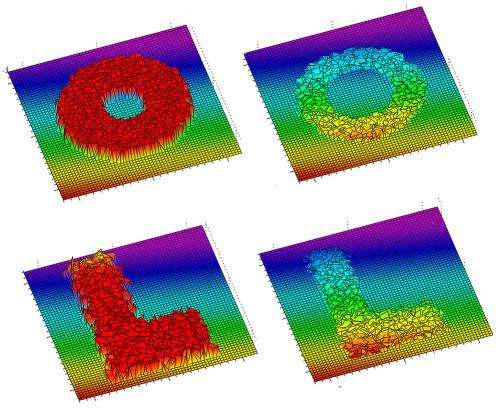
Folded DNA templates allow researchers to precisely cut out graphene shapes which could be used in electronic circuits

DNA's unique structure is ideal for carrying genetic information, but scientists have recently found ways to exploit this versatile molecule for other purposes: By controlling DNA sequences, they can manipulate the molecule to form many different nanoscale shapes.
Chemical and molecular engineers at MIT and Harvard University have now expanded this approach by using folded DNA to control the nanostructure of inorganic materials. After building DNA nanostructures of various shapes, they used the molecules as templates to create nanoscale patterns on sheets of graphene. This could be an important step toward large-scale production of electronic chips made of graphene, a one-atom-thick sheet of carbon with unique electronic properties.
"This gives us a chemical tool to program shapes and patterns at the nanometer scale, forming electronic circuits, for example," says Michael Strano, a professor of chemical engineering at MIT and a senior author of a paper describing the technique in the April 9 issue of Nature Communications.
Peng Yin, an assistant professor of systems biology at Harvard Medical School and a member of Harvard's Wyss Institute for Biologically Inspired Engineering, is also a senior author of the paper, and MIT postdoc Zhong Jin is the lead author. Other authors are Harvard postdocs Wei Sun and Yonggang Ke, MIT graduate students Chih-Jen Shih and Geraldine Paulus, and MIT postdocs Qing Hua Wang and Bin Mu.
Most of these DNA nanostructures are made using a novel approach developed in Yin's lab. Complex DNA nanostructures with precisely prescribed shapes are constructed using short synthetic DNA strands called single-stranded tiles. Each of these tiles acts like an interlocking toy brick and binds with four designated neighbors.
Using these single-stranded tiles, Yin's lab has created more than 100 distinct nanoscale shapes, including the full alphabet of capital English letters and many emoticons. These structures are designed using computer software and can be assembled in a simple reaction. Alternatively, such structures can be constructed using an approach called DNA origami, in which many short strands of DNA fold a long strand into a desired shape.
However, DNA tends to degrade when exposed to sunlight or oxygen, and can react with other molecules, so it is not ideal as a long-term building material. "We'd like to exploit the properties of more stable nanomaterials for structural applications or electronics," Strano says.
Instead, he and his colleagues transferred the precise structural information encoded in DNA to sturdier graphene. The chemical process involved is fairly straightforward, Strano says: First, the DNA is anchored onto a graphene surface using a molecule called aminopyrine, which is similar in structure to graphene. The DNA is then coated with small clusters of silver along the surface, which allows a subsequent layer of gold to be deposited on top of the silver.
Once the molecule is coated in gold, the stable metallized DNA can be used as a mask for a process called plasma lithography. Oxygen plasma, a very reactive "gas flow" of ionized molecules, is used to wear away any unprotected graphene, leaving behind a graphene structure identical to the original DNA shape. The metallized DNA is then washed away with sodium cyanide.
Shaping graphene circuits
The research team used this technique to create several types of shapes, including X and Y junctions, as well as rings and ribbons. They found that although most of the structural information is preserved, some information is lost when the DNA is coated in metal, so the technique is not yet as precise as another technique called e-beam lithography.
However, e-beam lithography, which uses beams of electrons to carve shapes into graphene, is expensive and takes a long time, so it would be very difficult to scale it up to mass-produce electrical or other components made of graphene.
One shape of particular interest to scientists is a graphene ribbon, which is a very narrow strip of graphene that confines the material's electrons, giving it new properties. Graphene doesn't normally have a bandgap—a property necessary for any material to act as a typical transistor. However, graphene ribbons do have a bandgap, so they could be used as components of electronic circuits.
"There is still interest in using graphene for digital electronics. Graphene itself isn't ideal for this, but if you pattern it into ribbons, it may be possible," Strano says.
Scientists are also interested in graphene rings because they can be used as quantum interference transistors, a novel type of transistor created when electrons flow around a circle. This type of behavior has only recently been observed, and this fabrication technique could allow scientists to create many rings so they can study this phenomenon more thoroughly.
In the longer term, the DNA nanostructure fabrication strategy could help researchers design and build electronic circuits made of graphene. This has been difficult so far because it's challenging to place tiny carbon structures, such as nanotubes and nanowires, onto a graphene sheet. However, using the metallized DNA masks to arrange structures on a sheet of graphene could make the process much easier.
The new approach is "conceptually novel," says Robert Haddon, a professor of chemical and environmental engineering at the University of California at Riverside, who was not part of the research team. "The work shows the potential of self-assembled metallized DNA nanoarchitectures as lithographic masks for wafer-scale patterning of graphene-based electronic circuit elements. I believe that this approach will stimulate further research on the application of nanopatterning techniques in graphene-based nanoelectronics."
Journal information: Nature Communications
Provided by Massachusetts Institute of Technology
This story is republished courtesy of MIT News (web.mit.edu/newsoffice/), a popular site that covers news about MIT research, innovation and teaching.


