Spanish scientists design a revolutionary data storage device

University of Granada researchers have developed a revolutionary data storage device in collaboration with the CEA-LETI lab at Grenoble (France), an institution of the Campus of International Excellence CEI BioTic. The researchers have designed one of the most advanced data storage devices in the world. The invention is protected with ten international patents including Japan, USA, Corea and the European Union. Important companies such as Samsung and Hynix (Corea) and Micron (USA) have shown interest in this innovative data storage device.
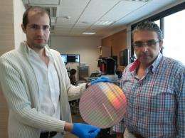
The researchers at the University of Granada Nanoelectronics Lab Noel Rodríguez and Francisco Gámiz have designed an Advanced Random Access Memory (A-RAM). The researchers developed the theoretical model of this new technology in 2009. The CEA-LETI lab –which has developed one of the most advanced nanoelectronic technologies in the world– have designed a device that experimentally confirms the results previously obtained in theoretical studies.
The results of this experimental validation have been published in the prestigious journal IEEE Electron Device Letters and were presented in the International Silicon on Insulator Technology Conference recently celebrated in San Francisco, USA.
In the wake of the new devices and microprocessors developed by Intel (Ivy Bridge), UGR scientists are investigating alternative 3D A2RAM-based memories such as FinFET-ARAM and Trigate-ARAM patented in France and presented in the International Memory Workshop celebrated in May 2012 in Milan, Italy.
Overcoming Challenges
University of Granada researchers have demonstrated that the memory cell A-RAM and its variant A2RAM can solve the miniaturization challenges in DRAM cells –which is the type of memory that most digital devices such as computers, smartphones, tablets, etc. incorporate- long retention times, low battery consumption, and a large separation between the logic levels, which makes it immune to noise/interferences and to the variability of technological processes.
According to Francisco Gámiz "since its invention in the 60's by Robert Dennard at IBM (USA), the commands and data necessary for the proper performance of a computer are stored as zeros (no charge) and ones (charge) in DRAM (Dynamic Random Access Memory) cell arrays". These cell arrays are composed of a transistor and a capacitor (ó 1T-1C-DRAM). Each bit of information is stored as an electric charge in a cell consisting on a transistor and a capacitor that provides access to the charge and, consequently, to the data.
Since its development, the DRAM concept has remained unchanged. Currently, we can find DRAM cells smaller than 20nm (1 nanometer is one billionth of a meter) and DRAM memory chips of several gigabytes (one gigabyte is one billion of bites). However, the possibilities of making these cells smaller are becoming exhausted due to the minimum charge needed to clearly distinguish between the two estates of a bit (1 and 0). This is drawing the line to the minimum size of capacitors. "If we cannot further reduce the size of the capacitor, the solution is to replace it with 1T-DRAM memory cells -or one-transistor memories- that store information directly in the transistor, which simultaneously detects the estate of the cells and gives access to the information stored."
More information
References:
N. Rodriguez, C.Navarro, F.Gamiz, F.Andrieu, O.Faynot, S.Cristoloveanu, "Experimental demonstration of A2RAM memory cells on Silicon-On-Insulator", IEEE Electron Device Letters, Aceptado para publicación (2012)
N.Rodriguez, C.Navarro, F.Gamiz, F.Andrieou, O.Faynot, S.Cristoloveanu, "Experimental Demonstration of A2RAM Memory Cell on SOI", IEEE International SOI Conference, San Francisco, Oct.2-4, 2012
F.Gamiz, N.Rodriguez and S.Cristoloveanu, "3D Trigate 1T-DRAM memory cell for 2x nmnodes",4th International Memory Workshop, Milan, May 20-22, 2012
Provided by University of Granada


