This article has been reviewed according to Science X's editorial process and policies. Editors have highlighted the following attributes while ensuring the content's credibility:
fact-checked
peer-reviewed publication
trusted source
proofread
Tweaking isotopes sheds light on promising approach to engineer semiconductors

Research led by scientists at the Department of Energy's Oak Ridge National Laboratory has demonstrated that small changes in the isotopic content of thin semiconductor materials can influence their optical and electronic properties, possibly opening the way to new and advanced designs with the semiconductors.
The work is published in the journal Science Advances.
Partly because of semiconductors, electronic devices and systems become more advanced and sophisticated every day. That's why for decades researchers have studied ways to improve semiconductor compounds to influence how they carry electrical current. One approach is to use isotopes to change the physical, chemical and technological properties of materials.
Isotopes are members of a family of an element that all have the same number of protons but different numbers of neutrons and thus different masses. Isotope engineering has traditionally focused on enhancing so-called bulk materials that have uniform properties in three dimensions, or 3D.
But new research led by ORNL has advanced the frontier of isotope engineering where current is confined in two dimensions, or 2D, inside flat crystals and where a layer is only a few atoms thick. The 2D materials are promising because their ultrathin nature could allow for precise control over their electronic properties.
"We observed a surprising isotope effect in the optoelectronic properties of a single layer of molybdenum disulfide when we substituted a heavier isotope of molybdenum in the crystal, an effect that opens opportunities to engineer 2D optoelectronic devices for microelectronics, solar cells, photodetectors and even next-generation computing technologies," said ORNL scientist Kai Xiao.
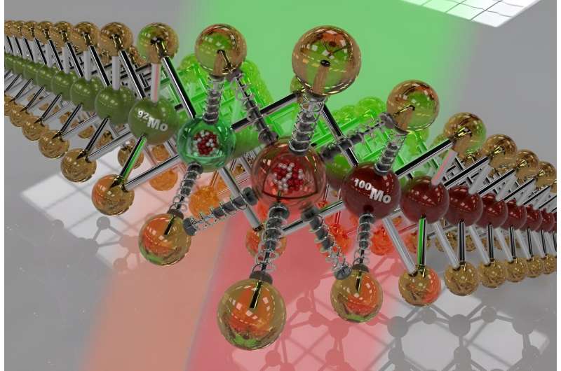
Yiling Yu, a member of Xiao's research team, grew isotopically pure 2D crystals of atomically thin molybdenum disulfide using molybdenum atoms of different masses. Yu noticed small shifts in the color of light emitted by the crystals under photoexcitation, or stimulation by light.
"Unexpectedly, the light from the molybdenum disulfide with the heavier molybdenum atoms was shifted farther to the red end of the spectrum, which is opposite to the shift one would expect for bulk materials," Xiao said. The red shift indicates a change in the electronic structure or optical properties of the material.
Xiao and the team, working with theorists Volodymyr Turkowski and Talat Rahman at the University of Central Florida, knew that the phonons, or crystal vibrations, must be scattering the excitons, or optical excitations, in unexpected ways in the confined dimensions of these ultrathin crystals.
They discovered how this scattering shifts the optical bandgap to the red end of the light spectrum for heavier isotopes. "Optical bandgap" refers to the minimum amount of energy needed to make a material absorb or emit light.
By adjusting the bandgap, researchers can make semiconductors absorb or emit different colors of light, and such tunability is essential for designing new devices.
ORNL's Alex Puretzky described how different crystals grown on a substrate can show small shifts in emitted color caused by regional strain in the substrate. To prove the anomalous isotope effect and measure its magnitude to compare with theoretical predictions, Yu grew molybdenum disulfide crystals with two molybdenum isotopes in one crystal.
"Our work was unprecedented in that we synthesized a 2D material with two isotopes of the same element but with different masses, and we joined the isotopes laterally in a controlled and gradual manner in a single monolayer crystal," Xiao said.
"This enabled us to observe the intrinsic anomalous isotope effect on the optical properties in the 2D material without the interference caused by an inhomogeneous sample."
The study demonstrated that even a small change of isotope masses in the atomically thin 2D semiconductor materials can influence optical and electronic properties—a finding that provides an important basis for continued research.
"Previously, the belief was that to make devices such as photovoltaics and photodetectors, we had to combine two different semiconductor materials to make junctions to trap excitons and separate their charges. But actually, we can use the same material and just change its isotopes to create isotopic junctions to trap the excitons," Xiao said.
"This research also tells us that through isotope engineering, we can tune the optical and electronic properties to design new applications."
For future experiments, Xiao and the team plan to collaborate with the experts at the High Flux Isotope Reactor and the Isotope Science and Engineering Directorate at ORNL. These facilities can provide various highly enriched isotope precursors to grow different isotopically pure 2D materials.
The team can then further investigate the isotope effect on spin properties for their application in spin electronics and quantum emission.
More information: Yiling Yu et al, Anomalous isotope effect on the optical bandgap in a monolayer transition metal dichalcogenide semiconductor, Science Advances (2024). DOI: 10.1126/sciadv.adj0758
Journal information: Science Advances
Provided by Oak Ridge National Laboratory


