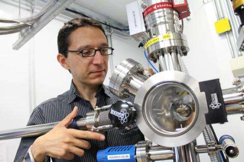
An interesting glimpse into how future state-of-the-art electronics might work

(Phys.org) —Using the Canadian Light Source (CLS) synchrotron, scientists have developed a new, cutting-edge technique enabling them to visualize the inner-workings of electronics.
This research is opening the door for a wide-range of opportunities for advanced nanoelectronics and devices. It could prove essential for the development of novel sensors for detecting light, magnetic fields and chemicals – which could be useful for medical analysis and treatments. New solar power harvesting capabilities might now be a step closer.
"We have been working on this project for several years, but the results are worth all the effort!" said lead investigator Prof. Vladimir Hinkov, from the Physics Institute and Röntgen Center at the University of Würzburg in Germany.
Computers, phones, and all electronic devices as we use them today are comprised of layers upon layers of nanometer-thin, conventional semiconducting films. A novel class of electronic materials – the so-called transition-metal oxides – hold promise for exciting, new applications. Where layers of this novel class of electronic materials touch, often a unique, and unprecedented phenomenon occurs: for instance, the interface between two insulators can become superconducting, or a strong magnetic order can build up between two non-magnetic layers.
A completely new class of electronic devices could be developed if scientists can understand the characteristics of these phenomena. Until recently, however, the properties of these films of novel materials have remained a mystery. This is mostly due to the fact that existing measurement techniques are either too coarse to reveal details on the atomic level, or because they destroy the film whilst trying to analyze it, impeding their ability to explain what was happening; until now.
An international team of researchers including members from the University of British Columbia, the Max Planck Institute for Solid State Research, University of Würzburg, the Leibniz Institute IFW, McMaster University, the University of California, and the CLS, developed a new technique based on resonant X-ray reflectivity that allows them to view these films at the atomic level: X-rays with a wavelength of a few nanometers are reflected off the different interfaces in the structure and subsequently overlap, pretty much as in holography using visible light. The resulting data then provides a depth-resolved picture of the structure.
This new, non-destructive technique has allowed scientists to finally see the building blocks of these new electronic materials up close for the first time. Visualizing the interfaces in layers of these materials will allow scientists to finally understand what makes them tick and consequently how to use them for greatly improved devices.
"An endeavour of this magnitude is only possible if colleagues with diverse fields of research are involved," said Prof. Hinkov. "Also, the required light has to be intense and of high quality, which can only be created in a synchrotron such as the Canadian Light Source."
Prof. Hinkov, who mainly focuses on fundamental physical questions, said that he could clearly see the next steps for their research. "We will investigate structures with interesting magnetic and electronic properties, and in the near future, colleagues who focus on electronics applications can use our results to develop components with tailored physical and technological properties."
Smart, innovative and highly sensitive technology could become a reality thanks to this innovative research.
More information: Macke, S., Radi, A., Hamann-Borrero, J. E., Bluschke, M., Brück, S., Goering, E., Sutarto, R., He, F., Cristiani, G., Wu, M., Benckiser, E., Habermeier, H.-U., Logvenov, G., Gauquelin, N., Botton, G. A., Kajdos, A. P., Stemmer, S., Sawatzky, G. A., Haverkort, M. W., Keimer, B. and Hinkov, V. (2014), Element Specific Monolayer Depth Profiling. Adv. Mater.. doi: 10.1002/adma.201402028
Provided by Canadian Light Source


