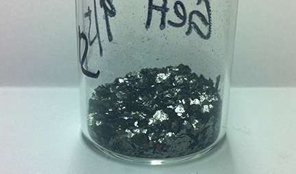
Thin layer of germanium may replace silicon in semiconductors

(Phys.org) —The same material that formed the first primitive transistors more than 60 years ago can be modified in a new way to advance future electronics, according to a new study.
Chemists at The Ohio State University have developed the technology for making a one-atom-thick sheet of germanium, and found that it conducts electrons more than ten times faster than silicon and five times faster than conventional germanium.
The material's structure is closely related to that of graphene—a much-touted two-dimensional material comprised of single layers of carbon atoms. As such, graphene shows unique properties compared to its more common multilayered counterpart, graphite. Graphene has yet to be used commercially, but experts have suggested that it could one day form faster computer chips, and maybe even function as a superconductor, so many labs are working to develop it.
Joshua Goldberger, assistant professor of chemistry at Ohio State, decided to take a different direction and focus on more traditional materials.
"Most people think of graphene as the electronic material of the future," Goldberger said. "But silicon and germanium are still the materials of the present. Sixty years' worth of brainpower has gone into developing techniques to make chips out of them. So we've been searching for unique forms of silicon and germanium with advantageous properties, to get the benefits of a new material but with less cost and using existing technology."
In a paper published online in the journal ACS Nano, he and his colleagues describe how they were able to create a stable, single layer of germanium atoms. In this form, the crystalline material is called germanane.
Researchers have tried to create germanane before. This is the first time anyone has succeeded at growing sufficient quantities of it to measure the material's properties in detail, and demonstrate that it is stable when exposed to air and water.
In nature, germanium tends to form multilayered crystals in which each atomic layer is bonded together; the single-atom layer is normally unstable. To get around this problem, Goldberger's team created multi-layered germanium crystals with calcium atoms wedged between the layers. Then they dissolved away the calcium with water, and plugged the empty chemical bonds that were left behind with hydrogen. The result: they were able to peel off individual layers of germanane.
Studded with hydrogen atoms, germanane is even more chemically stable than traditional silicon. It won't oxidize in air and water, as silicon does. That makes germanane easy to work with using conventional chip manufacturing techniques.
The primary thing that makes germanane desirable for optoelectronics is that it has what scientists call a "direct band gap," meaning that light is easily absorbed or emitted. Materials such as conventional silicon and germanium have indirect band gaps, meaning that it is much more difficult for the material to absorb or emit light.
"When you try to use a material with an indirect band gap on a solar cell, you have to make it pretty thick if you want enough energy to pass through it to be useful. A material with a direct band gap can do the same job with a piece of material 100 times thinner," Goldberger said.
The first-ever transistors were crafted from germanium in the late 1940s, and they were about the size of a thumbnail. Though transistors have grown microscopic since then—with millions of them packed into every computer chip—germanium still holds potential to advance electronics, the study showed.
According to the researchers' calculations, electrons can move through germanane ten times faster through silicon, and five times faster than through conventional germanium. The speed measurement is called electron mobility.
With its high mobility, germanane could thus carry the increased load in future high-powered computer chips.
"Mobility is important, because faster computer chips can only be made with faster mobility materials," Golberger said. "When you shrink transistors down to small scales, you need to use higher mobility materials or the transistors will just not work," Goldberger explained.
Next, the team is going to explore how to tune the properties of germanane by changing the configuration of the atoms in the single layer.
More information: dx.doi.org/10.1021/nn4009406
Journal information: ACS Nano
Provided by The Ohio State University


