This article has been reviewed according to Science X's editorial process and policies. Editors have highlighted the following attributes while ensuring the content's credibility:
fact-checked
peer-reviewed publication
trusted source
proofread
Unlocking the transformative potential of 2D materials to advance next-generation electronics

Van der Waals (vdW) dielectrics are widely used in nanoelectronics to preserve the intrinsic properties of two-dimensional (2D) semiconductors. However, achieving aligned growth of 2D semiconductors and their direct utilization on original vdWs epitaxial dielectrics to avoid disorders poses significant challenges.
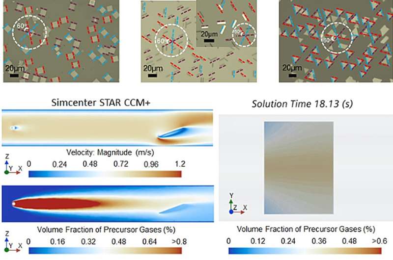
To overcome these challenges, researchers from the City University of Hong Kong (CityUHK) developed a hydromechanical strategy for aligned 2D material synthesis, pushing forward high-performance devices with as-grown 2D materials/vdWs dielectrics.
The findings, titled "Orientation-engineered 2D electronics on van der Waals dielectric," were published in the journal Matter.
"Directly utilizing 2D semiconductors on their as-grown substrates is significant in avoiding disorder-induced performance degradation of electronic devices. Our progress in this work ingeniously avoids the traditional material transfer process, which has substantial technological implications for unlocking the transformative potential of 2D materials," explained Professor Johnny Ho, Associate Vice-President (Enterprise) and Professor in the Department of Materials Science and Engineering at CityUHK, who led the study.

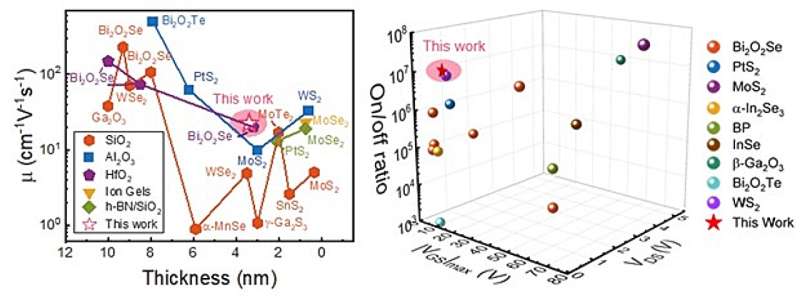
Leveraging the hydromechanical strategy developed in this study, the research team can control the preferential orientations of 2D materials on vdWs dielectrics. This breakthrough is highly significant, as it allows for the direct utilization of as-grown 2D materials on vdW dielectrics at the device level, minimizing the detrimental effects caused by disorder-induced performance degradation.
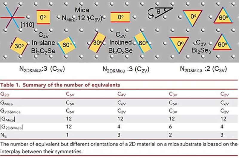
In addition, establishing the quantitative criterion for the epitaxy relationship with vdWs dielectrics can be aptly viewed as a measure of our understanding and can guide experimental decisions effectively. This finding opens up exciting opportunities for realizing next-generation electronics on vdW dielectric platforms.
The imperative to mitigate disorder-induced performance degradation in electronic devices has driven demand for the direct utilization of as-grown 2D materials/vdW dielectric. "However, the paradox is that the as-grown 2D materials are meticulously detached from the original substrates onto proposed dielectrics for further device fabrication," said Professor Ho.

With this powerful methodology platform for synthesizing aligned 2D materials, predicting alignment directions, and preserving their intrinsic properties, future research can leverage this knowledge to develop novel manufacturing techniques, enabling the production of high-performance electronic devices with enhanced functionality, reliability, and scalability. Such devices may include large-scale integrated circuits, flexible and wearable electronics, advanced optoelectronic devices, quantum technologies, etc.
Looking ahead, the research team aims primarily to transfer this technique to other 2D material systems to investigate their inherent properties and explore potential avenues for large-scale device integration. These endeavors aim to unlock further the transformative potential of aligned 2D materials on van der Waals dielectrics for developing innovative electronic devices.
More information: Weijun Wang et al, Orientation-engineered 2D electronics on van der Waals dielectrics, Matter (2024). DOI: 10.1016/j.matt.2024.04.013
Journal information: Matter
Provided by City University of Hong Kong


