This article has been reviewed according to Science X's editorial process and policies. Editors have highlighted the following attributes while ensuring the content's credibility:
fact-checked
peer-reviewed publication
proofread
Fundamental spatial limits of all-optical magnetization switching

Magnetization can be switched with a single laser pulse. However, it is not known whether the underlying microscopic process is scalable to the nanometer length scale, a prerequisite for making this technology competitive for future data storage applications.
Researchers at the Max Born Institute in Berlin, Germany, in collaboration with colleagues at the Instituto de Ciencia de Materiales in Madrid, Spain, and the free-electron laser facility FERMI in Trieste, Italy, have determined a fundamental spatial limit for light-driven magnetization reversal. The paper is published in the journal Nano Letters.
Modern magnetic hard drives can store more than one terabit of data per square inch, which means that the smallest unit of information can be encoded on an area smaller than 25 nanometers by 25 nanometers. In laser-based, all-optical switching (AOS), magnetically encoded bits are switched between their "0" and "1" state with a single ultrashort laser pulse. To realize the full potential of AOS, particularly in terms of faster write/erase cycles and improved power efficiency, whether a magnetic bit can still be all-optically reversed if its size is on the nanometer-scale needs to be understood.
For AOS to take place, the magnetic material has to be heated up to very high temperatures in order for its magnetization to be reduced close to zero. Only then, its magnetization can be reversed. The twist in AOS is that in order to mediate magnetic switching, it is sufficient to heat only the electrons of the material while leaving the lattice of atomic nuclei cold. This is exactly what an optical laser pulse does: it interacts only with the electrons, allowing to reach much higher electron temperatures with very low power levels.
However, since hot electrons cool very rapidly by scattering with the cold atomic nuclei, the magnetization must be reduced sufficiently fast within this characteristic time scale, i.e. AOS relies on a careful balance between the evolution of the electron temperature and the loss of magnetization. It is easy to see that this balance is changed when the optical excitation is confined to the nanoscale: now electrons can not only lose energy by "giving atomic nuclei a kick," but they can also simply leave the nanometer-small hot regions by diffusing away.
As they only have to traverse a nanometer-small distance in order to do so, this processes also happens on ultrafast time scale, such that the electrons may cool too quickly, the magnetization is not sufficiently decreased, and AOS breaks down.
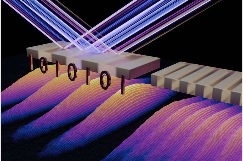
An international team of researchers has for the first time successfully addressed the question of "how small does AOS work" by combining experiments with soft X-rays with atomistic spin dynamics calculations. They produced an extremely short-lived pattern of dark and bright stripes of laser light at the sample surface of the prototypical magnetic material GdFe, by interference of two soft X-ray laser pulses with a wavelength of 8.3 nm.
This allowed reducing the distance between dark and bright areas to only 8.7 nm. This illumination is only present for about 40 femtoseconds, leading to a lateral modulation of hot and cold electron temperatures in the GdFe with a corresponding localized loss of magnetization.
The scientists could then follow how this pattern evolves on the very short time scales which are of relevance. Towards this end, a third soft X-ray pulse with the same wavelength of 8.3 nm was diffracted off the transient magnetization pattern at different time delays from the patter-generating pulses.
At this particular wavelength, an electronic resonance at the gadolinium atoms allows the soft X-ray pulse to "feel" the presence of magnetization and thus the change of the magnetization can be detected with femtosecond temporal and sub-nanometer spatial resolution. Combining the experimental results with state-of-the-art simulations, the researchers could determine the ultrafast energy transport on the nanometer scale.
It turns out that the minimum size for AOS in GdFe alloys, induced by a nanoscale periodic excitation, is around 25 nm. This limit is due to ultrafast lateral electron diffusion, which rapidly cools the illuminated regions on these tiny length scales and ultimately prevents AOS.
The faster cooling due to electron diffusion can be compensated to some extent by increasing the excitation power, but this approach is ultimately limited by the structural damage caused by the intense laser beam. The researchers expect that the 25 nm boundary is rather universal for all metallic magnetic materials.
More information: Felix Steinbach et al, Exploring the Fundamental Spatial Limits of Magnetic All-Optical Switching, Nano Letters (2024). DOI: 10.1021/acs.nanolett.4c00129
Journal information: Nano Letters
Provided by Max Born Institute for Nonlinear Optics and Short Pulse Spectroscopy (MBI)


