This article has been reviewed according to Science X's editorial process and policies. Editors have highlighted the following attributes while ensuring the content's credibility:
fact-checked
peer-reviewed publication
trusted source
proofread
Researchers realize orientation control of cMOF nanofilms

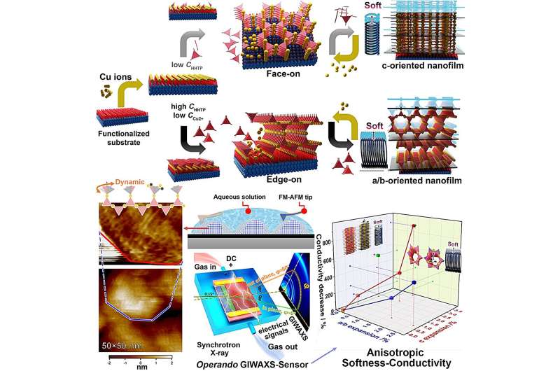
Researchers from the Institute of Process Engineering (IPE) of the Chinese Academy of Sciences and Kyoto University have proposed a strategy to grow "face-on" and "edge-on" conductive metal-organic frameworks (cMOF) nanofilms on substrates by controlling the "stand-up" behaviors of ligands on various surfaces to overcome the difficulty in the orientation control of such films.
They established operando characterization methodology using atomic force microscopy and X-ray to demonstrate the softness of the crystalline nanofilms and reveal their unique conductive functions. The study was published in Proceedings of the National Academy of Sciences on Sept. 25.
cMOFs have great potential for use in modern electrical devices due to their porous nature and the ability to conduct charges in a regular network. cMOFs applied in electrical devices normally hybridize with other materials, especially substrates. Therefore, precisely controlling the interface between a cMOF and a substrate is crucial.
However, the unexplored interface chemistry of cMOFs makes the controlled synthesis and advanced characterization of high-quality thin films particularly challenging. Specifically, in contrast to the anticipated "edge-on" alignment of the 2D planes stemming from the hydrophilic -OH edge and the hydrophobic triphenylene core, the orientation observed experimentally is, in fact, the "face-on" configuration of the 2D planes on the substrates.
"The challenge lies in inducing the necessary high surface pressure to achieve a 'standing up' configuration of the core," said Prof. Yao Mingshui from IPE, first author of the study.
In the Langmuir–Blodgett (LB) technique, ligands with a hydrophobic core and a hydrophilic edge can adopt an upright orientation on hydrophilic surfaces when subjected to high surface pressure.
"Inspired by the 'standing up' behaviors, we employ ultra-high concentration, together with vigorous evaporation during spraying, to create a unique local high surface pressure that can induce the 'standing up' of HHTP (HHTP = 2,3,6,7,10,11-hexahydrotriphenylene) ligands. Accordingly, the 'face-on' and 'edge-on' thin films can be fabricated," said Prof. Kenichi Otake from Kyoto University, corresponding author of the study.
Various reliable analyses were conducted to verify the crystallinity and orientation of the films with an ultra-thin thickness ranging from a few nanometers to tens of nanometers.
"The operando GIWAXS imaging and electrical monitoring revealed the anisotropic framework softness associated with electrical conductivity on the cMOF nanofilm. It answers the question whether the generally considered rigid Cu-HHTP can be soft," said Prof. Susumu Kitagawa from Kyoto University, corresponding author of the study. In addition to redox interactions, the structural softness has been confirmed to modulate the electrical conductivity in an anisotropic way.
More information: Ming-Shui Yao et al, Growth mechanisms and anisotropic softness–dependent conductivity of orientation-controllable metal–organic framework nanofilms, Proceedings of the National Academy of Sciences (2023). DOI: 10.1073/pnas.2305125120
Journal information: Proceedings of the National Academy of Sciences
Provided by Chinese Academy of Sciences


