This article has been reviewed according to Science X's editorial process and policies. Editors have highlighted the following attributes while ensuring the content's credibility:
fact-checked
peer-reviewed publication
trusted source
proofread
A platform for integrated spectrometers based on solution-processable semiconductors

Acquiring real-time spectral information in point-of-care diagnosis, internet-of-things, and other lab-on-chip applications requires spectrometers with hetero-integration capability and miniaturized features. Compared to conventional semiconductors integrated by heteroepitaxy, solution-processable semiconductors provide a much-flexible integration platform due to their solution-processability, and therefore, are more suitable for the multi-material integrated system. However, solution-processable semiconductors are usually incompatible with micro-fabrication processes, making them far from practical use in various lab-on-chip applications.
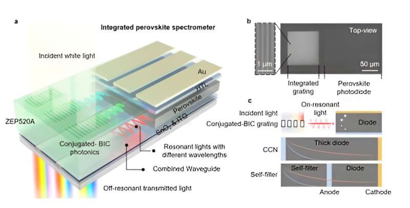
In a new paper published in Light: Science & Applications, a team of scientists led by Professor Qinghai Song from Ministry of Industry and Information Technology Key Lab of Micro-Nano Optoelectronic Information System, Guangdong Provincial Key Laboratory of Semiconductor Optoelectronic Materials and Intelligent Photonic Systems, Harbin Institute of Technology (Shenzhen), China have proposed a facile and universal platform to fabricate integrated spectrometers with solution-processable semiconductors by unprecedently involving the conjugated mode of bound states in the continuum (conjugated-BIC) photonics.
Specifically, exploiting the conjugated-BIC photonics, which remains unexplored in conventional lasing studies, renders the broadband photodiodes with ultra-narrowband detection ability, detection wavelength tunability, and on-chip integration ability while ensuring device performance. Spectrometers based on these ultra-narrowband photodiode arrays exhibit high spectral resolution and wide/tunable spectral bandwidth.
The fabrication processes are compatible with solution-processable semiconductors photodiodes like perovskites and quantum dots, which can be potentially extended to conventional semiconductors. Signals from the spectrometers directly constitute the incident spectra without being computation-intensive, latency-sensitive, or error-intolerant. As an example, integrated spectrometers based on perovskite photodiodes are capable of realizing narrowband/broadband light reconstruction and in-situ hyperspectral imaging. The reported platform provides insight into constructing integrated spectrometers with multi-material integrated systems.
"Exploring the conjugated-BIC is unconventional when compared with those popular BIC lasing studies. Through the theoretical study, we find that the conjugated-BIC experiences high leakage and decent Q while it can be easily excited and coupled. Considering that the conjugated-BIC photonics can be facilely fabricated and their resonant wavelengths can be effectively tuned, we anticipate that the conjugated-BIC is very suitable for wavelength-resolved photodetection applications," state the researchers.
"Solving the problems in fabricating perovskite photodiode arrays and integrating them with the conjugated-BIC photonics by micro-fabrication processes are also important since the materials and device interfaces of the devices can be easily destroyed during the processes by solvents and heat. We also believe that the photonics-optoelectronics integration platform we proposed can provide insight into broadening the functionalities and applications of the emerging solution-processable semiconductors like perovskites," the scientists conclude.
More information: Yanhao Li et al, A platform for integrated spectrometers based on solution-processable semiconductors, Light: Science & Applications (2023). DOI: 10.1038/s41377-023-01231-1
Journal information: Light: Science & Applications
Provided by Chinese Academy of Sciences


