July 31, 2023 feature
This article has been reviewed according to Science X's editorial process and policies. Editors have highlighted the following attributes while ensuring the content's credibility:
fact-checked
peer-reviewed publication
trusted source
proofread
Telecom-band-integrated multimode photonic quantum-memory

Quantum memory that depends on quantum-band integration is a key building block used to develop quantum networks that are compatible with fiber communication infrastructures. Quantum engineers and IT specialists have yet to create such a network with large capacity to form an integrated multimode photonic quantum memory at telecom band.
In a new report in Science Advances, Xueying Zhang and a research team in electronic science, physics, and information technology described fiber-integrated multimode storage of a single photon at telecom band on a laser-written chip.
The storage device made of fiber-pigtailed erbium (Er3+) doped lithium niobate (Er3+:LiNbO3), presented a memory system integrated with telecom-band fiber-integrated on-chip components. The outcomes of the study highlight a pathway for future quantum networks to come in to being, based on integrated photonics devices.
Photonic quantum memories
Quantum states of light can be mapped reversibly onto matter to create photonic quantum memories, ideal for long-distance quantum communication across distributed quantum networks.
Physicists have integrated optical waveguide-based photonic quantum memory devices with other integrated quantum devices such as a quantum light sources, photonic circuits, and single-photon detectors to engineer interconnected multifunctional quantum architectures. In this work, Zhang et al. developed a telecom-band-integrated multimode storage device in a lithium niobate-based waveguide.
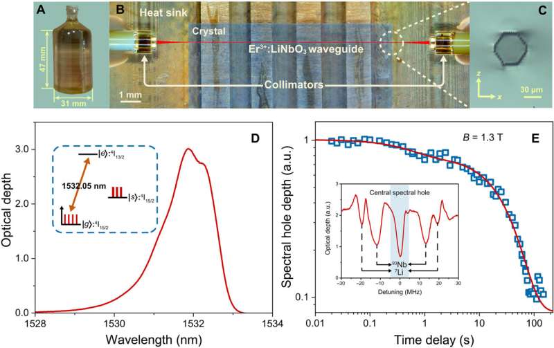
They engineered the laser-written waveguide with femtosecond laser micromachining directly coupled to a single-mode fiber pigtail by using an optical collimator on either side of the setup to facilitate compatibility with the fiber communication system.
The team developed an on-chip quantum memory system using an atomic frequency comb protocol. The integration of a 4 GHz-wide atomic frequency comb allowed the team to experimentally realize a multimode quantum storage system, paving the way to form integrated quantum networks with memory compatible with the infrastructure of fiber communication.

The experiments
Zhang et al. engineered a storge device using a type III waveguide fabricated in a wafer of erbium doped lithium niobate crystal by using femtosecond laser micromachining.
The bulk crystal of the material maintained a concentration of dopant ions at a minute percentage and allowed the coupling between laser-written waveguides and single-mode fibers. The scientists glued the doped lithium niobate crystal on a copper heat sink with two optical collimators with single-mode fiber pigtails.
They placed the fiber-integrated device in a dilution refrigerator and observed a total optical transmission frequency of 26 percent through the entire cryogenic setup.
Multimode storage
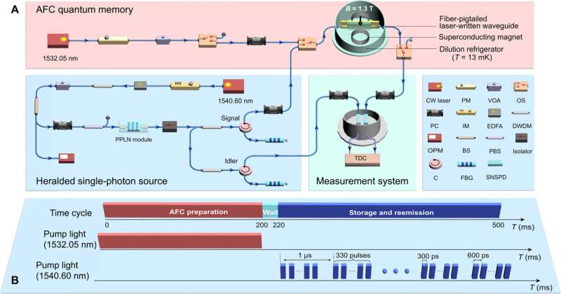
The experiments of multimode storage consisted of generating single photons to prepare the atomic frequency comb-based quantum memory and measurement system. The team generated correlated photon pairs by cascading second-harmonic generation and spontaneous parametric down conversion processes in the lithium niobate waveguide module pumped by a series of light pulses.
For the single-mode storage, the team used a single-laser pulse with a duration of 300 picoseconds. The scientists detected photons in the setup via superconducting nanowire single-photon detectors. Zhang et al. analyzed the detection signals of this instrument by using a time-to-digital converter.

Zhang and colleagues delivered the erbium (Er3+) ions into a periodic absorptive structure such as the atomic frequency comb with 5 MHz teeth spacing, which corresponded to a storage time of 200 nanoseconds. The team showed the storage of nonclassical light with a large time-bandwidth product.
They then sent the signal photons to the atomic frequency comb memory and calculated the efficiency of the system. Based on transmission efficiency of the memory device and spectral filtering of the input photons, they calculated the internal storage efficiency. The outcomes indicated the quantum memory of the atomic frequency comb to have maintained single-photon purity and spectral purity.
These outcomes led to Zhang et al. establishing an on-chip quantum memory with a storage time of 200 nanoseconds, while establishing negligible crosstalk in the instrument.

Outlook
In this way, Xueying Zhang and colleagues demonstrated an integrated multimode quantum memory-based on a laser written erbium doped lithium niobate waveguide. The team achieved a time-bandwidth product of 800, with a storage bandwidth of 4 GHz, and a storage time of 200 nanoseconds.
These outcomes in broadband multimode quantum storage will open the way to generate a high-rate quantum network. Although these results are significant, the researchers believe that several upgrades are needed to engineer a functional device to facilitate quantum networks.
The current approach integrates the reliability of a fiber-integrated device compatible with fiber telecom infrastructure to deliver promising, laser-written components with broadband multiplexed storage properties. The research team expect to combine photon pair sources with integrated memories to realize a high-rate quantum repeater protocol to create a large-scale quantum network.
These outcomes will help realize a quantum system with a large capacity, scalability, and compatibility of fiber communication towards the future impact and the construction of a global quantum network.
More information: Xueying Zhang et al, Telecom-band–integrated multimode photonic quantum memory, Science Advances (2023). DOI: 10.1126/sciadv.adf4587
Christoph Simon, Towards a global quantum network, Nature Photonics (2017). DOI: 10.1038/s41566-017-0032-0
Journal information: Nature Photonics , Science Advances
© 2023 Science X Network


