This article has been reviewed according to Science X's editorial process and policies. Editors have highlighted the following attributes while ensuring the content's credibility:

fact-checked

peer-reviewed publication

trusted source

proofread

Progressive quantum leaps—high-speed, thin-film lithium niobate quantum processors driven by quantum emitters
Progressive quantum leaps - high-speed thin-film lithium niobate quantum processors driven by quantum emitters
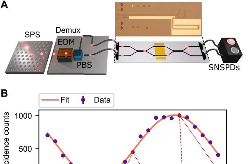
Measurement of on-chip quantum interference. (A) Schematic of the experimental setup. Photons generated by a QD SPS are sent into a two-mode demultiplexer consisting of a resonantly enhanced EOM and a polarizing beam splitter (PBS). The photons are subsequently collected into fibers and injected into the LNOI chip by a fiber array. Controlling the delay on one of the demultiplexer arms ensures that the photon pairs arrive at the device simultaneously, and fiber polarization controllers are used to optimize coupling into the TE mode. The output photons are collected via the same fiber array and routed to SNSPDs for coincidence detection. Inset: Image of the MZI device used. (B) Recorded coincidence data at zero time delay (shaded red areas in the insets) for varying applied voltages. Minima and maxima in the observed HOM fringe correspond to applied phases of ϕmin = π/2 + kπ and ϕmax = kπ, respectively, with k an integer number. The error bars are estimated from Poissonian statistics and are smaller than the data points. The HOM visibility of the quantum interference is determined from a curve fit (orange line) to be 92.7 ± 0.7%. Insets: Coincidence histograms for three different applied voltages. Credit: Science Advances (2023). DOI: 10.1126/sciadv.adg7268

Scalable photonic quantum computing architectures require photonic processing devices. Such platforms rely on low-loss, high-speed, reconfigurable circuits and near-deterministic resource state generators. In a new report now published in Science Advances, Patrik Sund and a research team at the center of hybrid quantum networks at the University of Copenhagen, and the University of Münster developed an integrated photonic platform with thin-film lithium niobate. The scientists integrated the platform with deterministic solid-state single photon sources using quantum dots in nanophotonic waveguides.

They processed the generated photons within low-loss circuits at speeds of several gigahertz and experimentally realized a variety of key photonic quantum information processing functionalities on high-speed circuits; with inherent key features to develop a four-mode universal photonic circuit. The results illustrate a promising direction in the development of scalable quantum technologies by merging integrated photonics with solid-state deterministic photon sources.

Advances in quantum technologies with integrated photonics

Quantum technologies have progressively advanced in the past several years to enable quantum hardware to compete with and surpass the capabilities of classical supercomputers. However, it is challenging to regulate at scale for a variety of practical applications and also to form fault-tolerant quantum technologies.

Photonics provide a promising platform to unlock scalable quantum hardware for long-range quantum networks with interconnections across multiple quantum devices and photonic circuits for quantum computing and simulation experiments. The high-quality photonic states and the fast, low-loss programmable circuits underlie the central idea of photonic quantum technologies to route and process applications. Researchers have recently developed solid-state quantum emitters such as as near-ideal, high-efficiency sources of indistinguishable photons to realize on-demand single-photon sources.
Progressive quantum leaps - high-speed thin-film lithium niobate quantum processors driven by quantum emitters
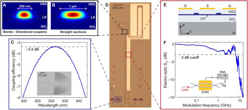
Overview of the platform. (A and B) Schematics of the designed waveguide geometry, tailored for the quantum emitter λ ≃ 940 nm operation wavelengths, for (A) SM waveguides used in bends and directional couplers, and (B) multimode straight waveguides. Color-coded is the field intensity of the fundamental TE waveguide mode. (C) Measured coupling efficiency of the fabricated grating couplers as a function of the input laser wavelength, with a peak efficiency of −3.4 dB. The inset shows a scanning electron micrograph image of the coupler. (D) Optical microscope image of an electrically tunable MZI. (E) Schematic of the cross section of the electro-optic phase shifter. (F) Modulation bandwidth of the MZI measured with a VNA. The data show a 3-dB cutoff at approximately 6.5 GHz. Inset, schematic of the setup used in the measurement. Credit: Science Advances (2023). DOI: 10.1126/sciadv.adg7268

Photonic quantum information processing

During this study, Sund and colleagues focused on single-crystal lithium niobate thin films bonded on a silica insulating substrate as a promising platform due to their strong electrical-optical properties, and high index contrast to form integrated circuits. Since the transparency range of the materials varied, they were well-suited to function with a variety of solid-state quantum emitters, with compatibility to function at cryogenic temperatures.

In this work, the team described the development of multimode lithium niobate on insulator circuits for quantum information processing at the single photon level for the first time. They accomplished this by using the circuits to regulate and facilitate the function of quantum states of light emitted from a quantum dot single-photon source. The team injected single photons emitted by a waveguide-integrated quantum dot source into the lithium niobate optical circuit to show key functionalities underlying photonic quantum information processing, such as multiphoton interference on a reconfigurable universal unitary circuit.
Progressive quantum leaps - high-speed thin-film lithium niobate quantum processors driven by quantum emitters
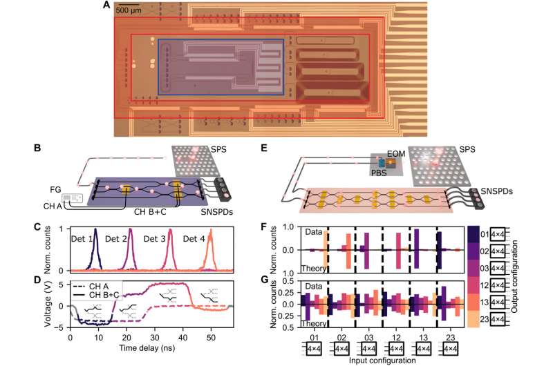
Photon processing in multimode high-speed integrated circuits. (A) Optical image of the chip. The photon router structure is highlighted in blue, and the 4 × 4 universal interferometer is highlighted in orange. (B) Schematic of the experimental setup used to perform active 1 × 4 demultiplexing of a stream of single photons produced by the QD. Photons are directly coupled in and out of the chip using a fiber array, and their time of arrival is recorded via SNSPDs and a time tagger. Fast electrical control is performed via a function generator (FG) connected to the modulators via a probe station, where a channel is used to individually address the MZI in the first layer and the other channel is split to drive both MZIs in the second layer in parallel. (C) Normalized photon counts in the four output waveguides within the time interval of a four-photon sequence. (D) Associated pulse sequences, with corresponding switching network configurations shown as insets. (E) Schematic of the experimental setup for the universal 4 × 4 interferometer. The 10 high-speed modulators used are electrically connected via a probe station and driven by a multichannel function generator. (F and G) Experimental data (top) and estimated theoretical (bottom) collision-free input-output probability distributions when programming the interferometer to implement an approximate permutation matrix (F) and a randomized unitary matrix (G), with estimated statistical fidelities of 96.3 and 95.5%, respectively. The horizontal index indicates the input configuration in terms of the mode indices of the first and second photon, and the color corresponds to the output configuration. Dashed lines separate different input configurations. Credit: Science Advances (2023). DOI: 10.1126/sciadv.adg7268

Integrated photonic platforms

Sund and colleagues illustrated the geometry used to realize single-mode lithium niobate on insulator waveguides. They implemented the optical circuits as rib waveguides via electron-beam lithography and argon etching on a lithium niobate film bonded on a silica-on-silicon substrate.

After etching them, they clad the waveguides with a hydrogen silsesquioxane layer and optically coupled the photonic integrated circuits to single-mode fibers for improved coupling efficiency for an active approach to interface fast optical switches and circuits with optical fibers. The and engineers realized the electro-optically tunable waveguide circuits with a Mach-Zehnder interferometer complete with directional couplers and an electrically tunable phase-shifter. The team tested the high-speed performance of the modulators to assess capabilities of the constructed photonic integrated circuits.

On-chip quantum interference

During photonic quantum information processing, the researchers investigated the visibility of multiphoton quantum interference through on-chip Hong-Ou-Mandel experiments to test the performance of the platform for photonic quantum information processing. The materials scientists generated single photons by using a self-assembled indium arsenide quantum dot embedded in a photonic and electronic nanostructure.

The device contained a single-sided photonic crystal waveguide and a shallow-etched waveguide grating for efficient photon generation alongside a hetero-diode for electrical noise suppression and emission wavelength tuning. The scientists created a two-photon input state from a stream of single photons emitted by the quantum dot, while using an off-chip demultiplexer to separate pairs of consecutive photons, allowing simultaneous arrival of the photons at the chip. They then routed the photons towards single-photon detectors for coincidence detection.
Progressive quantum leaps - high-speed thin-film lithium niobate quantum processors driven by quantum emitters
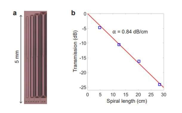
Measurement of the waveguide propagation loss. a Optical microscope picture showing the set of spirals employed for estimating the propagation loss of LNOI waveguides. b Measured transmission of the four spirals plotted in a dB scale (blue squares). The data are normalized to the transmission of a reference device consisting of only two grating couplers connected by a short waveguide. The red line is a linear fit (on the log scale) to the experimental data. Credit: Science Advances (2023). DOI: 10.1126/sciadv.adg7268

Integrated single-photon router

Fast photon routers are significant in photonic quantum computing, where they can be installed with multiple modes for multiplexing schemes in near-deterministic functions. Sund and colleagues made use of deterministic quantum emitters by rotating streams of emitted photons for networking schemes to reduce costs in photonic quantum computing architectures.

The research team integrated fast phase shifters on lithium niobate platforms and displayed on-chip routers for quantum-dot emitted photons. The demultiplexer in the experimental setup contained three fast electro-optic Mach Zehnder interferometer switches cascaded in a tree-shaped matrix network. The entire experimental circuit showed the promising potential of lithium niobate on the insulator platform to route photons produced by quantum dots.
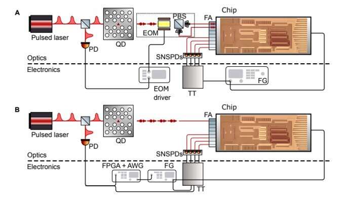
Progressive quantum leaps - high-speed thin-film lithium niobate quantum processors driven by quantum emitters
Schematics of full experimental setups. A. Schematic of the experimental setup used to perform measurements of two-photon interference in two-mode and four-mode interferometers. Optics: A pulsed laser operated at 72 MHz is used to drive a quantum dot (QD) single-photon source, producing a stream of single photons, which is routed into a two-mode demultiplexer consisting of an electro-optic modulator (EOM) and a polarizing beamsplitter (PBS). The demultiplexer splits subsequently emitted photons into two modes, one of which is delayed such that the photons are synchronized. The synchronized photons are subsequently sent to the chip via a fiber array (FA) and on-chip grating couplers, and extracted from different grating couplers and coupled to the same fiber array. The output photons are detected using superconducting nanowire single-photon detectors (SNSPDs) and the arrival times are recorded on a time-tagger (TT). Electronics: A fraction of the pulsed laser is split off using a beamsplitter and measured using a photodiode (PD). The resulting clock signal is used to trigger the EOM. A function generator (FG) is used to drive the modulators with an AC signal, and a synchronization signal is sent to the TT to allow for coincidence measurements between the control signal and single-photon detection events. B. Schematic of the experimental setup used to perform active 1 × 4 demultiplexing of a stream of single-photons produced by a quantum dot (QD) single-photon source. Optics: A pulsed laser operated at 72 MHz is used to drive a QD single-photon source, producing a stream of single photons. The stream of photons is routed directly into the chip via a fiber array (FA) and on-chip grating couplers, and output photons are extracted from different grating couplers with the same fiber array. These output photons are detected using superconducting nanowire single-photon detectors (SNSPDs) and the arrival times are recorded on a time-tagger (TT). Elecronics: A fraction of the pulsed laser is split off using a beamsplitter and measured using a photodiode (PD). Part of this clock signal is downsampled using a field-programmable gate array (FPGA) and used to trigger a square waveform with a repetition rate of ∼5 MHz on an arbitrary waveform generator (AWG). This ∼5 MHz signal is used to trigger a function generator (FG) which drives the modulators in an on-chip demultiplexer structure. A synchronization signal from the FG and the other part of the clock signal from the PD is sent into a time-tagger to enable coincidence detection between the input photon clock signal, the electronic control signal, and the single-photon detection events. Credit: Science Advances (2023). DOI: 10.1126/sciadv.adg7268

Universal four-mode interferometer

Multimode quantum photonic interferometers with programmable components are crucial to implementing core functionalities central to photonic quantum technologies such as multiphoton gates and fusion measurements to realize circuits for quantum computation experiments or for analog quantum simulation. The team explored the possibilities of quantum dot–lithium niobate on insulator platforms for this class of experiments and implemented an interferometer engineered from a network of six Mach Zehnder interferometers and ten phase modulators. The scientists then compared the measured distributions from experimental data with theoretical predictions.

Outlook

In this way, Patrik Sund and colleagues displayed the promise of lithium niobate on insulator platforms to process photons from emerging solid-state deterministic sources. The platform can be further optimized for scalable quantum technologies.

The team propose using a cladding with a higher refractive index during the experiments for optimized outcomes. The high-speed lithium niobate on insulator quantum processors provide a route to scale up quantum photonic technologies beyond photonic nanostructures—to achieve fault-tolerant photonic quantum computing at scale.

More information: Patrik I. Sund et al, High-speed thin-film lithium niobate quantum processor driven by a solid-state quantum emitter, Science Advances (2023). DOI: 10.1126/sciadv.adg7268

Han-Sen Zhong et al, Quantum computational advantage using photons, Science (2021). DOI: 10.1126/science.abe8770

Journal information: Science Advances , Science

© 2023 Science X Network

Citation: Progressive quantum leaps—high-speed, thin-film lithium niobate quantum processors driven by quantum emitters (2023, May 24) retrieved 25 April 2024 from https://phys.org/news/2023-05-quantum-leapshigh-speed-thin-film-lithium-niobate.html
This document is subject to copyright. Apart from any fair dealing for the purpose of private study or research, no part may be reproduced without the written permission. The content is provided for information purposes only.

Explore further

Wafer-scale nanofabrication of telecom single-photon emitters in silicon

136 shares

Feedback to editors