April 25, 2023 dialog
This article has been reviewed according to Science X's editorial process and policies. Editors have highlighted the following attributes while ensuring the content's credibility:
fact-checked
peer-reviewed publication
trusted source
written by researcher(s)
proofread
Van der Waals integration permits novel hetero-integrated photonic devices and flexible optical applications

Today, electronic and photonic devices are ubiquitous in smart phones, computers, light sources, sensors, and communications. To underpin the demand for optoelectronic applications, functional materials are essential. For instance, silicon is required for logic computing and photonic integrated circuits (PIC); group III-V semiconductors (such as GaAs, InP, AlN, etc.) are used for optoelectronic, light-emitting and photodetection applications; and piezoelectric materials are used for actuators and sensors.
However, the development of multifunctional and versatile photonic and optoelectronic systems would benefit from the realization of all the required functionalities using a single material platform. A heterogeneous integration platform has thus attracted tremendous interest from both academia and industry. Our research group (lead by Prof. Sang-Hoon Bae from Washington University in St. Louis, WUSTL) sought to address this need by using an advanced material epitaxy and layer transfer technique for novel optoelectronic applications.
The heterogeneous integration of functional materials and optical structures is essential for building high-performance integrated optoelectronic systems and an ideal platform for investigating nanophotonic phenomena. Conventional approaches to this rely on heteroepitaxy and require lattice-matching and process compatibility constraints. When the lattice constant differs more than a few percentage points between the epilayer and substrate, the grown films can be deteriorated by the polycrystalline phase or only epitaxial islands are formed, greatly degrading the intrinsic performance of the optical materials.
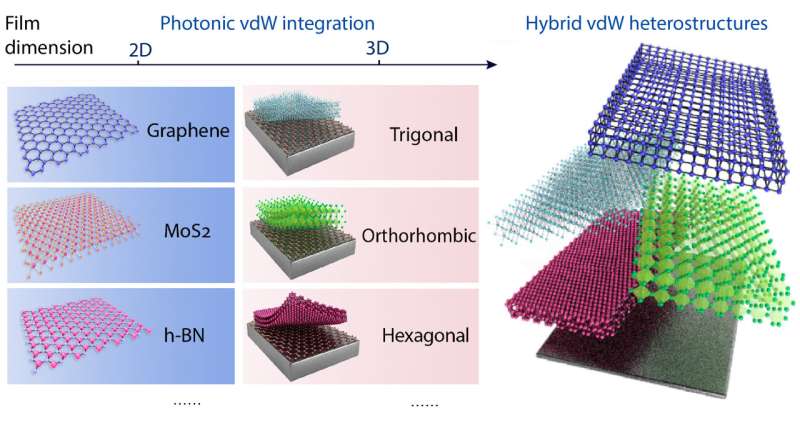
However, van der Waals (vdW) integration, leveraging isolated freestanding building blocks, is free of the lattice-matching constraints that apply in epitaxy. This low-energy physical assembly method was originally applied in two-dimensional materials due to its high flexibility in constructing vdW heterostructures (see figure above). Recent advances in advanced 2D-materials–assisted epitaxy and layer lift-off technologies have provided photonic engineers with many single-crystalline three-dimensional (3D) nanomembranes that can also be made to be ultrathin, flexible, and freestanding, like 2D materials. There has thus been exciting recent progress in optical and optoelectronic applications through photonic vdW integration.
In our recent paper published in Nature Reviews Materials, we presented a comprehensive catalog on the latest progress on photonic vdW integration from 2D materials to 3D nanomembranes, along with Prof. Cheng-Wei Qiu (National University of Singapore), Prof. Lan Yang (WUSTL), Prof. Jin-Wook Lee (Sungkyunkwan University), Prof. Yang Yang (University of California, Los Angeles) and other international collaborators. In addition to 2D materials, we also summarized currently available 3D freestanding nanomembranes. Detailed guidelines from thin film preparations to device implementations are outlined as well.
As the available material library of functional 3D nanomembranes is much wider than that of 2D materials, we thus envision emerging opportunities of van der Waals integration beyond 2D materials: High-quality, 3D thin films with exemplary functionalities such as optical gain, piezoelectric, electro-optical, and magneto-optical materials, etc., can be transferred to photonic structures to prototype novel devices and applications.
In this paper, we have also outlined promising opportunities for mixed-dimensional vdW heterostructures, advanced high-performance photonic devices based on novel hetero-integration layouts, and flexible and bio-compatible optoelectronic applications based on current perspectives. We also reviewed key technological challenges such as scalable nanomembranes manufacture and transfer for the field of thin-film photonics and photonic vdW integration.
This story is part of Science X Dialog, where researchers can report findings from their published research articles. Visit this page for information about ScienceX Dialog and how to participate.
More information: Yuan Meng et al, Photonic van der Waals integration from 2D materials to 3D nanomembranes, Nature Reviews Materials (2023). DOI: 10.1038/s41578-023-00558-w
Hyunseok Kim et al, Remote epitaxy, Nature Reviews Methods Primers (2022). DOI: 10.1038/s43586-022-00122-w
Yuan Liu et al, Van der Waals integration before and beyond two-dimensional materials, Nature (2019). DOI: 10.1038/s41586-019-1013-x
Journal information: Nature
Dr. Yuan Meng is a Postdoctoral Research Associate in the Department of Mechanical Engineering and Materials Science, Washington University in St. Louis, USA. Dr. Sang-Hoon Bae is Assistant Professor at the Department of Mechanical Engineering and Materials Science, Washington University in St. Louis, USA.


