December 1, 2021 feature
Developing wafer-scale highly oriented graphene on sapphire

Researchers have used direct chemical vapor deposition (CVD) growth of wafer-scale, high-quality graphene on dielectrics for versatile applications. However, graphene synthesized this way has shown a polycrystalline film with uncontrolled defects, a low carrier mobility, and high street resistance; therefore, researchers aim to introduce new methods to develop wafer-scale graphene. In a new report now published in Science Advances, Zhaolong Chen and an international research team in nanochemistry, intelligent materials and physics, in China, U.K. and Singapore, described the direct growth of highly oriented monolayer graphene on films of sapphire wafers. They achieved the growth strategy by designing an electromagnetic induction CVD at elevated temperature. The graphene film developed in this way showed a markedly improved carrier mobility and reduced sheet resistance.
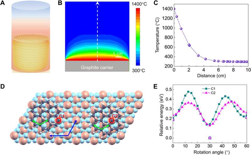
The development and applications of graphene on materials.
Graphene has a good mechanical robustness, a high carrier mobility, increased optical transparency and holds promise for high-frequency applications, as well as transparent conductive electrodes. The linear dispersion of the Dirac electrons of graphene can also allow target devices including photodetectors and optical modulators. Most such applications rely on the use of single-crystal, wafer-scale graphene without contamination or breakages. While wafer-scale, high-mobility graphene was readily produced before, the layer number uniformity has remained unsatisfactory across the entire wafer. Researchers therefore sought to facilitate the direct synthesis of graphene on silicon oxide, hexagonal boron nitride (hBN), and glass by using conventional chemical vapor deposition techniques. In this work, Chen et al. presented the direct growth of wafer-scale continuous, highly oriented monolayer graphene films on sapphire via an electromagnetic induction-heating-based method of chemical vapor deposition. This approach of direct growth of highly oriented graphene films on sapphire wafers paved the way towards emerging graphene electronics and photonics.

The experiments: Graphene on sapphire
During the experiments, Chen et al. used electromagnetic induction heating as the heat source of the chemical vapor deposition (CVD) system to extend the growth parameter space during the growth of high-quality graphene. The reactor enabled quick temperature ramping to 1400 degrees Celsius within 10 minutes. The process allowed precise regulation on the active carbon supply for the homogenous growth of monolayer graphene. To understand the role of sapphire during graphene formation, the team conducted density functional theory (DFT) calculations to reveal the preferred orientation of the graphene domain on sapphire. To accomplish this, they modeled the adsorption of a small graphene cluster (C24H12) on an aluminum oxide slab. The model showed the possibility for the growth of wafer-scale highly oriented graphene on sapphire, after an interface coupling-guided growth mechanism. The elevated temperature during growth facilitated sufficient pyrolysis of methane and the efficient migration of the adsorbed active carbon on sapphire to promote the growth rate and crystal quality. A continuous graphene film covered the 2-inch sapphire wafer within 30 minutes with high transparency.

Characterizing the graphene film on the sapphire wafer
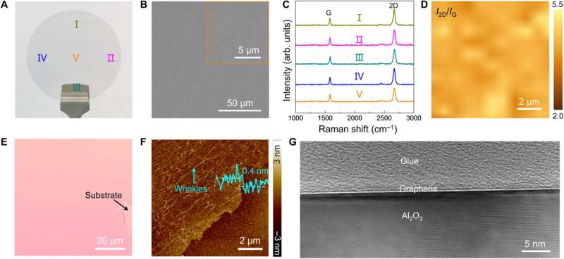
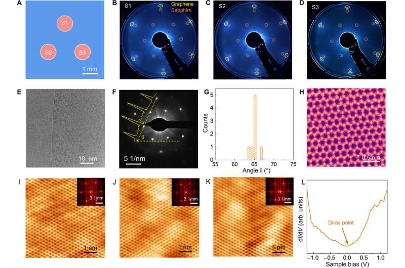
Using scanning electron microscopy (SEM), Chen et al. noted a homogenous contrast of the monolayer graphene at full coverage, without any voids. Using Raman spectra of the graphene produced on sapphire, they identified Raman signals indicative of a high quality monolayer of graphene and confirmed its uniformity across the wafer scale. The optical microscopy results similarly showed a uniform optical contrast without any contamination or visible secondary layers. Using atomic force microscopy, they then identified further characteristics of monolayer graphene grown by the CVD (chemical vapor deposition) method. Further analysis with transmission electron microscopy (TEM) showed high uniformity without contamination. The experimental setup allowed the growth of monolayer graphene in the absence of large carbon clusters in the gas phase and the presence of individual carbons reaching the surface of graphene to quickly migrate to the edge of graphene. To understand the lattice orientations of the as-grown monolayer of graphene on sapphire, the team performed low-energy electron diffraction characterization and revealed the highly oriented nature of the wafer-sized graphene. To further verify structural information of the material, they conducted selected area electron diffraction measurements and also noted the honeycomb lattice architecture of graphene using atomically resolved TEM images. The experimental setup allowed the nuclei to reach the most stable orientation.

Further experiments
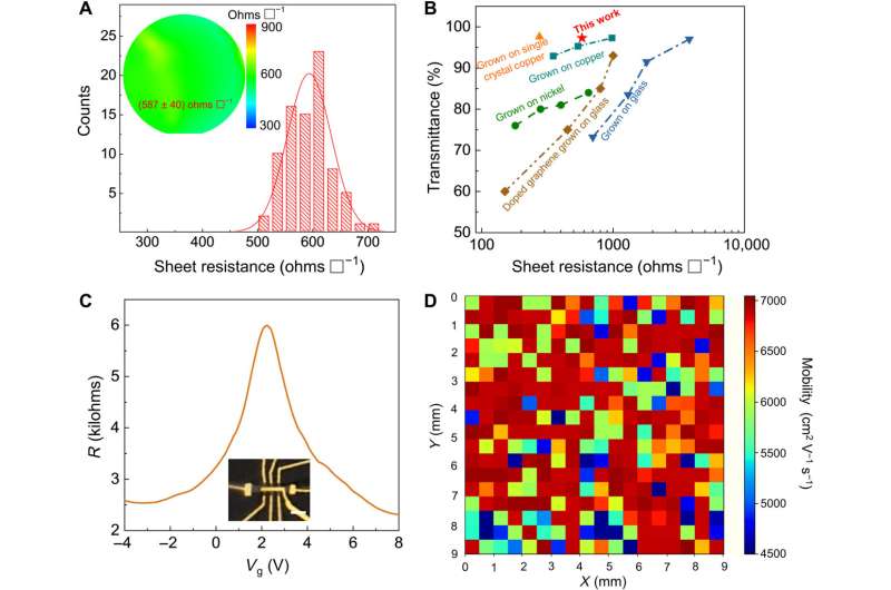
Chen et al. next conducted scanning tunneling microscopy (STM) to probe the stitching state of the graphene domains. The STM image revealed a honeycomb lattice, too, aligned without any defects. The atomically resolved image further highlighted the presence of a continuous film with a small grain boundary. The work also confirmed the successful climbing of sapphire steps caused by carbon thermal reduction of sapphire. The V-shaped density states alongside the characteristic Dirac cone-like feature of single-layer graphene agreed with the honeycomb architecture to re-establish the high quality and purity of the highly oriented film of thus grown graphene. The scientists next performed macroscopic four probe transport measurements to assess the large-scale electrical conductivity of as-grown high-quality graphene on sapphire wafers. They noted a sheet resistance map of a 2-inch graphene/sapphire wafer, with an average value as low as 587 ± 40 ohms. The outcome was markedly superior when compared to those for graphene directly grown on glass substrates. The team then measured the field-effect mobility of graphene on sapphire and recorded its carrier density. The values were also markedly higher than those observed with graphene directly grown on dielectric substrates and metals. The outcomes hold promise in electronic and optoelectronic applications.
Outlook
In this way, Zhaolong Chen and colleagues developed a method for the direct growth of wafer-scale, continuous, highly oriented monolayer graphene film on sapphire using an electromagnetic induction heating CVD route. The synthetic method facilitated quick temperature ramping up to 1400 Celsius within 10 minutes for efficient pyrolysis of carbon feedstock to enable the fast migration of active species. This efficient and reliable synthetic route of high-quality monolayer graphene on sapphire wafer was compatible with semiconductor processes and can ultimately promote high-performance graphene electronics and industrialization.
More information: Zhaolong Chen et al, Direct growth of wafer-scale highly oriented graphene on sapphire, Science Advances (2021). DOI: 10.1126/sciadv.abk0115
Yanqing Wu et al, High-frequency, scaled graphene transistors on diamond-like carbon, Nature (2011). DOI: 10.1038/nature09979
Journal information: Science Advances , Nature
© 2021 Science X Network


