November 16, 2021 feature
Borophenes made easy
. (A) Schematic of diborane dosage on the preheated Ir(111) surface to obtain borophene. (B) STM image of a single-crystalline borophene domain grown by CVD on Ir(111) (Vbias = 0.1 V). (C) Detailed structure of borophene whose unit cell is depicted in red (Vbias = 2.0 V). (D) Schematic of sequential borazine and diborane dosage to obtain borophene-hBN lateral heterostructures. (E) High-resolution STM image of the lateral heterostructure formed by borophene and hBN (Vbias = 1.2 V). Red lines highlight χ6 borophene’s wavy appearance, and green solid and dashed rhomboids highlight the unit cell and hexagonal moiré pattern of hBN, respectively. (F) XPS boron and nitrogen 1s core levels measured on borophene. (G) Schematic of the vertical heterostructure, with hBN covering borophene, grown by sequential dosing. (H) Atomically resolved image of the hBN lattice covering the borophene in the vertical heterostructure. (Vbias = 0.10 V; subtle 3D rendering was applied for better visualization). (I) Mass spectra of diborane and borazine gas used to grow borophene and hBN, respectively, measured at partial pressure of 3 × 10⁻⁷ mbar. Credit: Science Advances, doi: 10.1126/sciadv.abk1490")
Synthetic organic chemists still aim to understand the scalable synthesis of elemental, two-dimensional (2D) materials beyond graphene. In a new report, Marc G. Cuxart and a team of researchers in physics, chemistry and electrical and computer engineering in France and Germany, introduced a versatile method of chemical vapor deposition (CVD) to grow borophenes and borophene heterostructures via the selective use of diborane originating from traceable byproducts of borazine. The team successfully synthesized metallic borophene polymorphs on Iridium (IR) (III) and Copper (Cu) (III) single-crystal substrates alongside insulating hexagonal boron nitride (hBN) to form atomically precise lateral borophene—hBN interfaces. This structure protected borophene from immediate oxidation due to the presence of a single insulating hBN overlayer. This direct approach and ability to synthesize high-quality borophenes with large single-crystalline domains via chemical vapor deposition can open a range of opportunities to study their fundamental properties. The work is now published in Science Advances.
Synthesis of borophenes
The ability to synthesize 2D materials without naturally occurring layered analogs has opened a new path to property engineering based on the choice of constituent elements and the design of in-plane atomic structures. The elemental layers of different 2D synthetic materials are stabilized by strong covalent bonds. Borophenes offer interesting anisotropic, electronic and mechanical properties to yield control on properties and emerging functionalities. These outcomes have driven experimental efforts to synthesize stable 2D polymorphs of boron known as borophenes. In 2015, researchers synthesized atomically thin borophenes by depositing borons from high-purity solid sources onto the surface of a silver single-crystal in ultrahigh vacuum, following a physical vapor deposition method. Scientists then applied this procedure across varied surfaces, but the lack of a suitable boron precursor to prompt 2D nucleation and growth was a major impediment to produce atomically thin borophenes. In this work, Cuxart et al. therefore identified diborane (B2H6) in commercial borazine, based on previous studies. Using diborane as a molecular precursor of the high quality growth of atomically thin borophene layers, they developed an easy and regulated CVD route to form unprecedented vertical and lateral heterostructures. The work opens a new path to explore borophene properties in van der Waals heterostructures and devices.
. (A) High-resolution STM image of the atomically sharp heterointerface formed by borophene and hBN (Vbias = − 0.5 V). Subtle 3D rendering was applied for better visualization. The interfacial registry is highlighted by the red and green lines. (B) dI/dV spectra taken on borophene and hBN rim and valley regions, together with (C) simultaneously acquired I(V) curves (stabilization conditions: Vbias = 1.5 V, It = 0.25 nA, lock-in modulation voltage V = 50 mV). The borophene spectra represent an average over the unit cell. (D) dI/dV intensity map constructed from the series of dI/dV spectra measured along the blue line marked on the STM image (Vbias = 2.0 V) showing a sharp electronic transition. Spectra stabilized at Vbias = 1.5 V and It = 0.4 nA, lock-in modulation voltage V = 50 mV. STM images measured at (E) Vbias = 2.7 and (F) Vbias = − 0.8 V, showing a bias-dependent contrast inversion between borophene and hBN. Credit: Science Advances, doi: 10.1126/sciadv.abk1490")
Experiments and characterization.
During the study, Cuxart et al. dosed diborane onto a preheated, atomically clean and flat surface after selectively filtering from borazine by applying a freeze-thaw cycle to the precursor dosing system. During borazine synthesis, amine borane formed a major intermediate to act as a source for diborane. The team credited the presence and continuous reformation of diborane to an ongoing decay of inherent or acquired trace impurities in the commercial borazine precursor, widely used for hBN monolayer synthesis. The scientists then characterized the resulting material using low-temperature scanning tunneling microscopy (STM) and X-ray photoelectron spectroscopy (XPS). The STM images showed a "wavy" pattern by dosing diborane on iridium. To develop borophene using this method, Cuxart et al. introduced a versatile method of chemical vapor deposition. The XPS characterization indicated the borophene polymorph grown by chemical vapor deposition to confirm the presence of boron and the absence of nitrogen. The team studied the combined growth of borophene and single-layer hBN as a multifunctional, insulating 2D material.
Examining borophene-hBN heterostructures
-
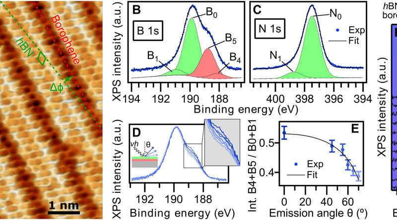
hBN on borophene: vertical heterostructure on Ir(111). (A) Atomically resolved STM image of an hBN domain, featuring its honeycomb structure, on χ6 borophene, showing its stripy appearance on Ir(111) (hBN unit cell in green, Vbias = 1.0 V). Subtle 3D rendering has been applied for better visualization. Inset: LEED pattern acquired at 79 eV (simulated diffraction pattern of hBN in green and borophene in red). (B) Boron and (C) nitrogen 1s XP spectra. The fitted components of hBN and borophene spectral contributions are displayed in green and red, respectively. (D) B 1s peak measured at different photoelectron emission angles θ = 0°, 45°, 55°, 60°, 65°, and 70° (lines from dark to light blue). (E) Angular dependence of the relative intensity of borophene B 1s components and Beer-Lambert law fit in black describing the attenuation effect by the hBN overlayer. (F) Series of B 1s spectra measured on hBN-covered borophene after incremental O2 exposure intervals reveals no sign of oxidation in contrast to an uncovered borophene sample that shows emergence of oxidized boron (G). Intensity maps at the background are constructed with the presented spectra. Credit: Science Advances, doi: 10.1126/sciadv.abk1490 -
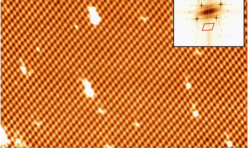
CVD growth of borophene on Cu(111). (A) STM image of a single-crystalline χ3-like borophene domain (Vbias = 1.3 V). Top right inset shows a fast Fourier transform of the image. The scan area is highlighted in the bottom left inset (tunneling current channel, Vbias = 1.3 V). (B and C) High-resolution STM images of the same borophene domain recorded at Vbias = 0.5 and −3.0 V, respectively. Black vectors indicate the unit cell. Credit: Science Advances, doi: 10.1126/sciadv.abk1490
The scientists further noted the formation of a straight and sharp 1-D interface supported by an atomic-scale description of the bonding configuration by using density functional theory. The outcome was also observed experimentally via the atomically resolved STM (scanning tunneling microscopy) image. The team showed how electron transitions from borophene to hBN occurred without an apparent interface state, which Cuxart et al. identified using scanning tunneling spectra (STS). They then developed additional methods to produce a borophene-hBN heterostructure by dosing 1.8 L of diborane and 4.5 L of borazine onto iridium. The doses corresponded to the growth of a full monolayer of borophene and hBN on iridium surfaces. Using scanning tunneling microscopy, they obtained a hBN honeycomb structure to then indicate weak interactions between hBN and borophene. The weak diffraction points further demonstrated the alignment of the borophene superstructure with the hBN cover. To prevent the oxidation of borophene that can otherwise limit its stability upon exposure to air, Cuxart et al. investigated the protective capping effect that inert hBN conferred to borophene. To study this, the team measured X-ray photoelectron spectra on hBN-covered and uncovered borophene—after exposing the surfaces to incremental doses of molecular oxygen at room temperature. In contrast to bare borophene, the hBN-covered borophene remained completely unchanged, to highlight the impact of hBN as a protective layer against oxidation of borophene.
Growth of borophene on copper and the overall outlook
To understand the effects of chemical vapor deposition (CVD) across diverse metallic substrates, Cuxart et al. also studied the growth of borophene on copper (Cu) (III), a weaker interacting support. In this instance, they dosed 18 l of diborane onto a copper single crystal kept at 773 K. The scientists then characterized the resulting material to reveal the presence of single-crystalline domains. In this way, by choosing both copper and iridium surfaces, Marc G. Cuxart and colleagues showed how similar structures could be formed via different approaches. The outcomes verified the possibility of using the CVD method to deliver boron, to generate borophenes and heterostructures with hBN. The work further supported the possibility of using the chemical vapor deposition route to form borophene polymorphs based on diborane as a source of boron. The team stressed the importance of high purity precursors to selectively deposit single phases. The method can be used on diverse substrates to open a path for the in-situ growth of heterostructures based on low-dimensional materials that protect borophene from oxidation. This approach can open a range of methods to study the fundamental aspects of synthetic 2D materials for technically relevant applications.
More information: Marc G. Cuxart et al, Borophenes made easy, Science Advances (2021). DOI: 10.1126/sciadv.abk1490
Andrew J. Mannix et al, Borophene as a prototype for synthetic 2D materials development, Nature Nanotechnology (2018). DOI: 10.1038/s41565-018-0157-4
Journal information: Science Advances , Nature Nanotechnology
© 2021 Science X Network


