June 13, 2019 feature
Visualizing a quantum crystal: Imaging the electronic Wigner crystal in 1-D

When electrons that repel each other are confined to a small space, they can form an ordered crystalline state known as a Wigner crystal. Observing the fragile crystal is tricky, since it requires extreme conditions including low temperatures and densities, as well as noninvasive imaging probes. To overcome the challenging conditions of imaging, I. Shapir and a research team in the departments of Physics and Condensed Matter Physics in Israel, Romania and Hungary created conditions in a carbon nanotube (NT) to house the electrons. They followed this experimental step by using a second nanotube as a probe (called "probe NT") to scan the first nanotube (termed "system NT"). The physicists measured the electronic densities and showed their consistency with theoretical predictions to demonstrate small Wigner crystals of up to six electrons in one dimension (1-D). The results are now published in Science.
More than 80 years ago, physicist Eugene Wigner predicted the quantum crystal of electrons, which remains one of the most elusive states of matter. In the present work, Shapir and co-workers developed a technique to directly image the Wigner crystal in 1-D by imaging its charge density in real space. They obtained images of a few electrons confined in 1-D that matched the theoretical predictions for strongly interacting crystals. The scientists viewed the quantum nature of the crystal using collective tunneling through an electric potential barrier confined with electrically independent gates. The work provided direct evidence to the formation of small Wigner crystals, paving the way to study fragile interacting states of electrons by imaging their many-body density in real space.
In his 1934 paper, physicist Eugene Wigner predicted that when long-range Coulomb interactions in a system of electrons dominated the kinetic energy and disorder, they would emerge in a crystalline ground state. Where the electrons were kept apart irrespective of their quantum number . Experimental physicists began to search for this quantum crystal in the cleanest available electronic systems thereafter, including liquid helium and low-dimensional semiconductor heterostructures.

Physicists had previously conducted measurements in two-dimensional (2-D) electronic systems relative to transport, microwave fields, nuclear magnetic resonance, optical, tunneling and bilayer electron systems to indicate the existence of a crystal at high magnetic fields. Observing a crystalline state in one-dimension (1-D), in an infinite system is unexpected, since thermal and quantum fluctuations can destroy long-range order. However, in finite systems, physicists had studied the theoretical one-dimensional Wigner crystal state since the quasi-long-range order produced crystalline correlations. Experimental physicists followed this observation with experimental probing via transport measurements, but the experiments could only probe macroscopic properties of this state.
In principle, a suitable imaging tool is required to observe the unambiguous fingerprint of a Wigner crystal in its real-space structure. Scientists therefore used scanning probe experiments, although they could only image the non-interacting state or show invasive gating by the probe. The measurements highlighted the inherent difficulty of imaging electron interactions with conventional scanning methods. To individually resolve and identify electrons, a macroscopic, metallic or dielectric tip should approach the electrons closer than their mutual separation. Nevertheless, such tips and their interactions can strongly distort the state being studied. Scientists therefore required a different scanning probe to image an interacting state or electron system.

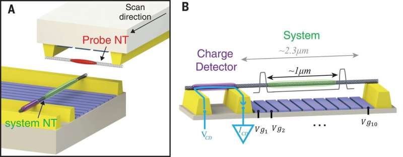
In the present work, Shapir et al. introduced a scanning probe platform that used a carbon nanotube (NT) as a highly sensitive, yet minimally invasive scanning probe to view the many-body density of strongly interacting electrons. The platform contained a custom-made scanning probe microscope operating at cryogenic temperatures (~10 mK) where two opposing NT devices could be brought in close proximity and scanned along each other. The scientists used one device to host the system NT as the 1-D platform under study, and the second device perpendicularly to that to contain the probe NT. They assembled the two devices using a nanoassembly technique to form pristine NTs suspended above an array of metallic gates.
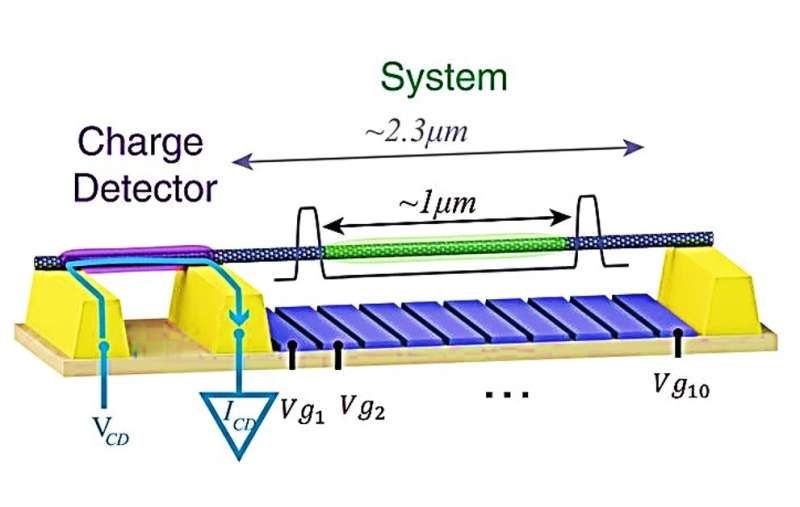
The scientists crucially maintained strong interactions and low disorder in the system to obtain a Wigner crystal by suspending the NTs far above the metallic gates at 400 nm. Then using 10 electrically independent gates they designed a potential that confined the electrons between two barriers 1 µm apart, localizing them centrally in a long suspended nanotube, away from contacts to prevent undesirable interactions.
Shapir et al. used highly opaque barriers to prevent hybridization of the confined electron's wave function with those of the electrons in the rest of the NT. Since transport in this situation was highly suppressed, the scientists probed the confined electrons using a charge detector located on a separate segment of the same NT. The probe NT device separately used in the study maintained an almost identical structure, which only differed by the suspension length of 1.6 µm and the number of gates (three).

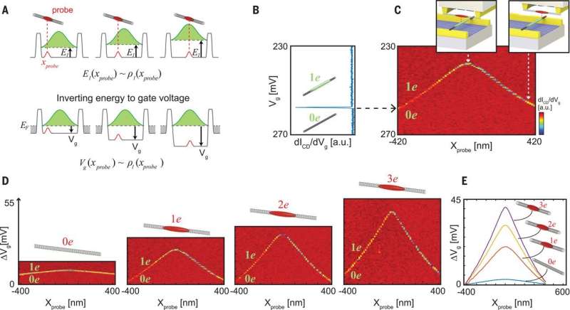
The scientists demonstrated the working principle underlying the imaging technique known as the "scanning charge," starting with the simplest experiments on imaging the charge distribution of a single electron confined in a 1-D box. Shapir et al. measured the energetic response of the system to a scanned perturbation (agitation) and directly determined the system's density distribution. By measuring the system's energy as a function of the probe NT, the scientists directly resolved the electron's density profile. When measuring the energy, the scientists referenced it to the Fermi energy in the leads and credited the perturbation produced by the probes to the separation between the two NTs and to the confined charge within the probe NT.
![Many-body tunneling of the few-electron state. (A) Illustration of the potential landscape, which now includes a central barrier through which an electron can tunnel (red arrow). The detuning voltage, ε, changes the relative height of the bottom of each well. (B) Charge stability diagram for 1e as a function of Vg and ε, measured using dICD/dε (color bar). The states (N, M) denote the charge N (M) in the left (right) wells. The vertical, wider line corresponds to an internal tunneling, occurring when EN+1,M = EN,M+1. (C) Schematic of the expected tunneling differential density for one electron (red “dipole”, bottom), given by the difference between its density distribution before and after tunneling [ρ10(x) and ρ01(x)] convolved with the probe’s point spread function (PSF). (D) Measured charge detector signal as a function xprobe and the difference in detuning relative to the unperturbed state, Δε. The red trace shows the Δε(xprobe) necessary to keep the tunneling in resonance (shown schematically in inset), giving the tunneling differential density. (E) Same as (A), but for three electrons in the trap. (F) Two scenarios for the tunneling: (Left) Only the central electron moves in the tunneling event; Δε(xprobe) will show a single dipole, as in the one-electron case illustrated in (C). (Right) Many-body tunneling, in which the coordinates of all the electrons move coherently in the tunneling process; multiple dipoles are expected in the differential tunneling signal. (G) (Top inset) Charge-stability diagram of three electrons, with ICD/dε (a.u.) measured for −42 mV < ε < 10 mV, 170 mV < Vg < 130 mV. (Main panel) Measured Δε(xprobe) for three electrons, exhibiting multiple dipoles. (Bottom inset) DMRG-calculated many-body density distributions of three electrons that the electrons tunnel between (blue and red) and their difference, convolved with the probe’s PSF (blue, bottom), showing that all electrons move a fraction of their zero-point motion as part of the many-body tunneling. Credit: Science, doi: 10.1126/science.aat0905. Visualizing a quantum crystal – Imaging the electronic Wigner crystal in 1-D](https://scx1.b-cdn.net/csz/news/800a/2019/4-visualizinga.jpg)
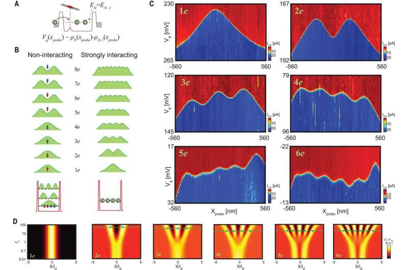
Shapir et al. obtained six panels in the experiments to indicate the differential density of the six electrons added to the system NT. For minimal perturbations, they performed all scans with one electron in the probe NT. The imaged density profiles clearly differed from those predicted by single-particle physics yet matched those of a strongly interacting crystal. When Shapir et al. increased the number of electrons, the electron spacing reduced, although their overall speed increased to signify electrons confined in a "box" with soft walls. The resulting images provided direct, real-space observations of the electronic Wigner crystals.
To quantitatively understand the measurements, Shapir et al. performed density matrix renormalization group (DMRG) calculations and included long-range Coulomb interactions. The measured electron positions (viewed as green stars) agreed well with those predicted by DMRG, placing the observed crystals well within the strongly interacting regime in the experimental setup. To understand the quantum nature of the Wigner crystal, Shapir et al. measured the tunneling characteristics of the crystal and expected the correlations between the electrons in a crystal to cause the crystal to tunnel through a barrier collectively. They observed the tunneling differential density become more interesting in a system with more than one electron since it displayed direct fingerprints of collective motion.
In this way, Shapir et al. used a new method to directly image the spatial ordering of interacting electrons. Based on the results, they anticipate the possibility of addressing additional basic questions related to the quantum electronic crystal, including the nature of its magnetic ordering. The scanning platform developed by Shapir et al. will allow further exploration of a much wide range of canonical interacting electron states of matter that were previously beyond imaging reach.
More information: I. Shapir et al. Imaging the electronic Wigner crystal in one dimension, Science (2019). DOI: 10.1126/science.aat0905
E. Wigner. On the Interaction of Electrons in Metals, Physical Review (2002). DOI: 10.1103/PhysRev.46.1002
J. Waissman et al. Realization of pristine and locally tunable one-dimensional electron systems in carbon nanotubes, Nature Nanotechnology (2013). DOI: 10.1038/nnano.2013.143
L. Tiemann et al. NMR profiling of quantum electron solids in high magnetic fields, Nature Physics (2014). DOI: 10.1038/nphys3031
Journal information: Science , Nature Nanotechnology , Nature Physics
© 2019 Science X Network


