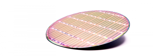
Imec presents back-side illuminated CMOS image sensor with UV-optimized antireflective coating

At this week's VISION 2014 exhibition, imec presents a backside-illuminated (BSI) CMOS image sensor chip featuring a new anti-reflective coating (ARC) optimized for UV light. Targeting imaging solutions in new markets such as life sciences, the achievement is an important addition to imec's customized 200mm CMOS fab. This 200mm process line enables imec to offer design, prototyping and low volume manufacturing of custom specialty chip solutions such as highly specialized CMOS image sensors.
Known for its superior enhanced light sensitivity compared with image sensors using front side illumination (FSI), BSI sensors are top candidates to further improve the performance of CMOS image sensors. Widely spread today in consumer applications such as smart phones, BSI imagers are expected to enter the higher-end application space of e.g. industrial inspection.
BSI imagers have a clear advantage when it comes to fill factor for the pixel area, angular response, and the complete avoidance of absorption or scattering losses in the metal interconnect layers. The cost for these light gathering improvement are the extra process complexity for the backside fabrication and possible electrical and optical losses at the new backside silicon interface. Therefore the engineering of the backside layers and interfaces is key to develop high performance BSI devices
Imec is tackling these challenges to exploit the benefits of BSI imagers for highly specialized customized imagers for space applications, high speed cameras, semiconductor inspection and medical applications,... To minimize reflection losses and maximize transmission of light to the sensor, specific anti-reflective coatings (ARC) are developed for various applications targeting different regions of the light spectrum. The coatings are applied at wafer level as part of the BSI process flow.
Imec has already developed an ARC for visible light range (400nm-800nm) with >70% QE over the entire spectral range. Imec's new ARC, targeting the UV range, shows excellent performance at near UV wavelengths, with Quantum Efficiency (Q.E.) values above 50 percent over the entire spectral range from 260nm to 400nm wavelength.
"This is an important milestone for imec's customized 200mm CMOS process line, demonstrating our expertise and capability to design, prototype and manufacture high-end CMOS image sensors," said Rudi Cartuyvels, senior vice president, Smart Systems & Energy Technologies at imec. "The development widens our portfolio towards new markets, offering solutions for both visible and UV imaging in semiconductor equipment applications, such as advance lithography and wafer and mask inspection."
Provided by IMEC


