Creating nanostructures using simple stamps

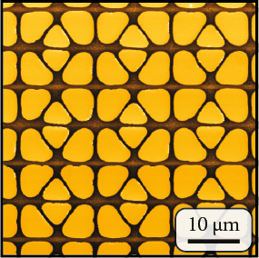
Nanostructures of virtually any possible shape can now be made using a combination of techniques developed by the MESA+ Institute for Nanotechnology of the University of Twente. Especially the unique properties of so-called perovskites can be exploited further: their crystal structure is not influenced by the process. The UT scientists present their findings in the journal Advanced Functional Materials.
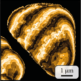
Perovskites are materials with special properties, especially at their interfaces. At the interface between two non-conducting perovskites, for example, a conducting 'path' can arise. The magnetic properties of perovskites are unique as well. Within the group Inorganic Materials Science, UT scientists have gained a lot of experience with these materials: earlier, the group developed the Pulsed Laser Deposition technique(PLD) for this, building the materials one atomic layer at a time. PLD is now combined with another technique, for creating patterns within these ultra thin layers. This was a problem until now, because other patterning techniques have the risk of damaging the crystal structure and orientation and thus influence the properties of the material. The new combination of techniques does not show this disadvantage.
Simple mold
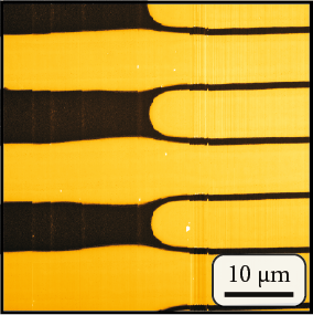
The solution that UT researchers publish in Advanced Functional Materials is combining PLD with so-called soft lithography. The mold used for creating patterns, can be made relatively easy and consists of PDMS – a rubber like polymer with silicon in it. Via this mask, a pattern of zinc oxide can be placed on the perovskite, for example. Using PLD, a sandwich of different materials can be made. The properties of each layer are secured. The new structures can lead to sensors and chips for future devices like smartphones, computers and medical equipment. They are also suitable for fundamental research in physics and materials science.

Research has been done within the Inorganic Materials Science group, part of the MESA+ Institute for Nanotechnology at the University of Twente.
The paper 'Patterning of epitaxial perovskites from micro and nano molded stencil masks' by Maarten Nijland, Antony George, Sean Thomas, Evert Houwman, Jing Xia, Dave Blank, Guus Rijnders, Gertjan Koster en André ten Elshof will appear in Advanced Functional Materials. The paper is online as an 'Early View' and will appear in one of the coming issues.

More information: Nijland, M., George, A., Thomas, S., Houwman, E. P., Xia, J., Blank, D. H. A., Rijnders, G., Koster, G. and ten Elshof, J. E. (2014), "Patterning of Epitaxial Perovskites from Micro and Nano Molded Stencil Masks." Adv. Funct. Mater.. doi: 10.1002/adfm.201401170
Journal information: Advanced Functional Materials
Provided by University of Twente


