November 17, 2011 report
Light-controlling artificial diamond structures could lead to optical computers

(PhysOrg.com) -- In an effort to make computer chips even faster than those of today, many researchers have recently been investigating the possibility of optical computing. In an optical computer, information is encoded as photons rather than electrons, allowing large amounts of data to be processed simultaneously. But before an optical computer can be realized, researchers need to design a 3D structure that can sufficiently manipulate light. Electronic computers switch electric current on and off using semiconductors with band gaps for electrons, in which electric current is forbidden to pass through. By analogy, optical computers are expected to require optical semiconductors with photonic band gaps, in which light of a range of wavelengths is forbidden to pass through.
Manufacturing 3D structures that can control light in this way is difficult, since the technology currently used to manufacture today’s computer chips involves building the structures on the chip layer by layer. This technique would be time-consuming and expensive for fabricating 3D optical chips.
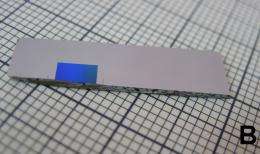
But recently, a team of researchers from the Netherlands led by Professor Willem Vos from the MESA+ Institute at the University of Twente, the University of Eindhoven, the ASML company, and the TNO Institute has for the first time fabricated 3D structures with a photonic band gap that can control the emission of light. The 3D structures are photonic crystals that possess an artificial diamond structure, which is etched in a silicon wafer using CMOS-compatible methods.
“For a complete photonic band gap, it is crucial to have 3D structures at one’s disposal,” University of Twente researchers Willem Tjerkstra, Léon Woldering, and Vos told PhysOrg.com. “Our work is the first ever demonstration of the radical control of the spontaneous emission of light by means of a photonic band gap (while electronic band gaps are known for a long time, there is no such thing as ‘spontaneous emission of current’).”

Precise etching
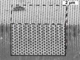
The researchers described how to fabricate these 3D structures in two recent studies. Starting with crystalline silicon wafers, the researchers first etched a set of pores in a rectangular pattern on the top surface of the wafers. To do this, they used advanced deep-UV lithography, in which a giant camera uses UV light to project the pore structure onto the silicon surface. This light created an etch mask with millions of tiny pores. Then the researchers used a plasma etching process that is commonly used in the computer chip industry to deeply etch nanopores into the silicon wafer.
Next, the researchers etched a set of pores in the same rectangular pattern on the thin side of the wafer, so that this set of pores crossed the first set of pores at a 90° angle. Although the researchers used the same standard equipment to etch the side pores as the top pores, it was much more difficult due to the extreme precision required. The mask pattern had to be aligned as accurately as possible in order for the pores to be correctly, perpendicularly aligned with the first set.
As the researchers explained, this fabrication process involves two significant advances: it consists of only two etching steps, and it does not require any specialized equipment. The team reported the development of the precise etching technique in a paper published in the Journal of Vacuum Science and Technology. In a second paper, published in Advanced Functional Materials, they reported applying the technique to make the 3D photonic crystals with artificial diamond structures.

“The central result of the Tjerkstra, et al., article [1] is the fact that we have, for the first time, developed a way to realize 3D nanostructures in silicon by making etch-masks on two different sides of a wafer,” the researchers said. “The accuracy with which the two etching masks are aligned is unprecedented: the mask patterns are aligned to within a distance of 30 nm and within an angle of 0.5° of the optimal configuration. As a result, a complex 3D structure can be made in only two etching steps, instead of tediously making such a structure by stacking layer-by-layer, as in standard CMOS-compatible fabrication.
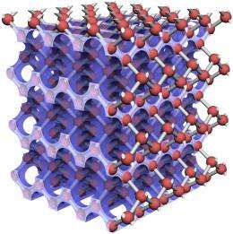
“The central result of the van den Broek, et al., paper [2] is that we have employed our 3D etch-masking method to realize a complex 3D periodic array (a crystal structure) of pores in silicon. The intersections of the pores are ordered in the same way as atoms in a diamond crystal. As the pores are spaced by several hundred nanometers, the structure is a photonic crystal, that is, a metamaterial that radically modifies the propagation and emission of light.”

This diamond structure is what gives the structure its photonic band gap, which is required for future optical computers. Theoretically, the 3D structure reflects 100% of incoming light of a certain wavelength, although in reality the maximum reflectivity is limited by the roughness and the size of the crystal. Also, the band gap appears at the near-infrared wavelengths between 1330 and 1550 nm, which are used in the telecommunications industry, making the structure appear promising for applications. Since the methods involved are compatible with standard chip-technology, the researchers hope that the optical structures can be easily integrated with existing electronic computer chips.
Optical computers
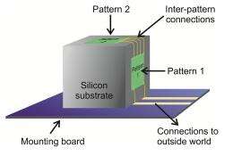
To use these structures to manipulate data in an optical computer, the researchers will need to integrate a cavity inside the highly reflective 3D structures to capture photons. Inside this “cage for light,” light will continually bounce between the walls of the cage until it is “set free” by the press of a button. In this way, the cavity will serve as an optical one-bit memory, although researchers are still discussing how to optically define “ones” and “zeros.” Integrating such a cavity into the 3D structures will require additional nanofabrication methods. The researchers noted that similar cavities have already been made in 2D photonic crystals, although the light can leak out by escaping in the third dimension.
Ultimately, these steps could lead to the development of an optical computer that can process far more data simultaneously than a conventional computer. Because the components on an optical device must operate at a certain size set by the wavelength of light, they would not be governed by Moore’s law. According to Moore’s law, the number of transistors on an electronic computer chip doubles approximately every two years, meaning more computing power per chip area.
“Moore’s Law - in the sense of miniaturizing devices to pack them in a higher density - does not apply to photonic components because when photonic crystals become smaller their properties change: If one were to make crystals smaller by removing unit cells, their ability to manipulate light diminishes, and if one would make the feature sizes smaller, the wavelengths of the photonic band gap in the electromagnetic spectrum decrease (typically to ranges where light is absorbed),” the researchers explained.
“If one were able to control and manipulate information in the form of optical bits, this has an important feature, namely that much more information can be handled simultaneously than with well-known electronic schemes. The reason is that light can be modulated at a much higher frequency than electronic systems (typically 100 to 1000 times faster), on account of its much higher natural frequency. Whether this will lead to a new type of ‘Moore’s law’ is not known at this time.”
In addition to computing, the new 3D structures could have other optical applications. For instance, in a third paper [3], the researchers demonstrated for the first time the inhibition of the spontaneous emission of light. Predicted 25 years ago by American scientists, this phenomenon provides a new way to control transitions of electrons inside atoms or molecules, and could lead to enhanced semiconductor LEDs, solid-state lasers, and solar cells. The results may also serve to shield sensitive quantum systems from ubiquitous noise as a result of vacuum fluctuations of light.
“There are other important applications that can be addressed with the new results,” the researchers said. “For instance, new nanophotonic know-how is leading to unconventional ways to realize microscopy with unprecedented resolution. And our methods and techniques are also expected to yield much more efficient LEDs and ‘green technology,’ as this will allow mankind to considerably save on power consumption while simultaneously allowing for much higher comfort and well-being for many more people on our beautiful planet.”
More information: [1] R.W. Tjerkstra, L.A. Woldering, J.M. van den Broek, F. Roozeboom, I.D. Setija, and W.L. Vos. “A method to pattern etch masks in two inclined planes for three-dimensional nano- and microfabrication.” Journal of Vacuum Science and Technology B. (soon online)
[2] J. M. van den Broek, L. A. Woldering, R. W. Tjerkstra, F. B. Segerink, I. D. Setija, and W. L. Vos. “Inverse-Woodpile Photonic Band Gap Crystals with a Cubic Diamond-like Structure Made from Single-Crystalline Silicon.” Adv. Funct. Mater. 2011. DOI:10.1002/adfm.201101101
[3] M. D. Leistikow, A. P. Mosk, E. Yeganegi, S. R. Huisman, A. Lagendijk, and W. L. Vos, “Inhibited spontaneous emission of quantum dots observed in a 3D photonic band gap.” Phys. Rev. Lett. 107, 193903: (2011). DOI: 10.1103/PhysRevLett.107.193903
Journal information: Advanced Functional Materials
© 2011 PhysOrg.com


