Processing technology to improve the electrical properties of glass ceramic circuit boards

As you ease your foot off the accelerator, a radar sensor detects how far away you are from the other cars and intelligently adjusts your speed appropriately. Technology like this is already helping to improve road safety and is set to become even more commonplace. From an electrical engineering perspective, manufacturing sensors of this kind is an extremely tricky process: the sensors have to be able to operate at very high frequencies but still need to be precise and efficient. TU Wien has now managed to develop a new processing technology for the high-precision nanostructuring of glass ceramic circuit boards. This means that the material properties can be adjusted, thereby significantly improving the electromagnetic behaviour of the sensor.
The material affects the radiation properties
Radar sensor antennas have very little in common with the metal rods that you might see protruding from a radio set. That is because today's sensor antennas are extremely compact and mounted directly onto the circuit boards. The circuit boards themselves can, for example, be made from special glass ceramics (called 'low-temperature co-fired ceramics' or 'LTCC') comprising various layers with the PCB tracks mounted in between. The patch antenna is located on the top layer.
'The radiation characteristic of an antenna is heavily influenced by the underlying material,' explains Prof. Ulrich Schmid from the Institut für Sensor- und Aktuatorsysteme at TU Wien (the Institute for Sensor and Actuator Systems at TU Wien). Depending on the electromagnetic properties of the circuit board, the material may interfere with the radiation process and absorb the waves being emitted. In extreme cases, it may even heat up to such an extent that the semiconductor chips are also affected. This is particularly problematic in the high-frequency range: car radar sensors operate at around 77 GHz for a mixture of technical and legal reasons, with this frequency range having been specifically reserved by law for radar sensors used in road traffic applications.
Attempts have already been made to prevent the material from interfering by combining the circuit board glass ceramics with organic materials. However this brings with it a whole new set of problems. 'It is best to avoid transitions between different materials,' says Ulrich Schmid. Situations involving different categories of material that expand to different extents when they heat up are particularly likely to shorten the life span of the radar sensor.
The nanopore technique
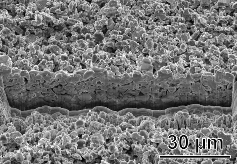
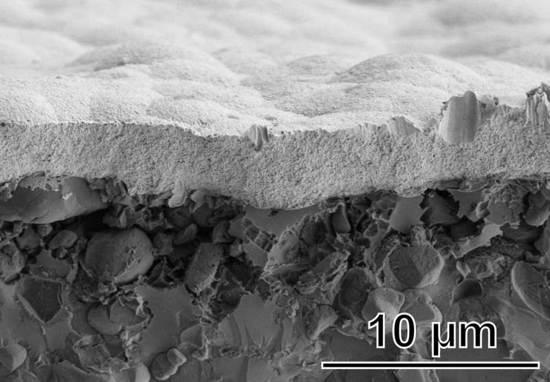
For the reasons outlined above, researchers at TU Wien decided to look for a way of changing the electromagnetic properties of the circuit boards in a very specific manner without having to use an additional material. The glass ceramics consist of tiny grains that are 'welded together' by heat. This baking process produces feldspar, which can be etched away using acid, leaving behind the rest of the substrate material. What the research team discovered was that this technique could be used to provide the glass ceramic material with a complex pore structure at a nanolevel, thereby changing the properties of the material at specific points.

The extent to which a material can be penetrated by electrical fields is referred to as its 'electrical permittivity'. 'Prior to the acid treatment, the permittivity measures between seven and eight but the nanopores reduce it by up to 30%. Not only that, but this can be achieved with a minimum of technological effort and using conventional tape systems that were not even produced with this etching process in mind. That is impressive,' exclaims Dr. Achim Bittner. Bittner studied this effect several years ago and now his colleague Frank Steinhäußer has managed to develop the technique further in conjunction with Happy Plating (an electroplating company based in Austria) with very promising results. The remaining steps required to manufacture the antenna circuit board were carried out by partners in Germany. For instance, the glass ceramics were sintered by MSE using material supplied by Kerafol. The high-frequency simulations were performed and the antenna was designed at the University of Erlangen-Nuremberg and by Astyx.
The new etching technique can be used with pinpoint accuracy to imbue different parts of the glass ceramics with different properties. This may – for example – prove extremely useful in the context of multi-antenna arrays that are connected for the purpose of transmitting an electromagnetic wave in a very specific direction. There are also plans to use the technique as a diagnostic method in the future to find out more about the behaviour of the glass ceramic material with a view to improving it further at a fundamental level.
Provided by Vienna University of Technology


