Researchers introduce new layered semiconducting materials as silicon alternative

When the new iPhone came out, customers complained that it could be bent—but what if you could roll up your too big 6 Plus to actually fit in your pocket? That technology might be available sooner than you think, based on the work of USC Viterbi engineers.
For many decades, silicon has been the heart of modern electronics—but as a material, it has its limits. As our devices get smaller and smaller, the basic unit of these devices, a transistor, must also get tinier and tinier. Bottom line: the size of the silicon transistor is reaching its physical limit. As silicon devices are based on what is called a top-down cutting method, it is increasingly difficult for silicon to be made even smaller. Consumers also demand phones to be lighter, faster, smaller, more flexible, wearable, bendable, etc. Yet silicon is also rigid—one can't bend your smart phone or computer. These physical limitations have driven the race for new materials that can be used as semiconductors in lieu of silicon.
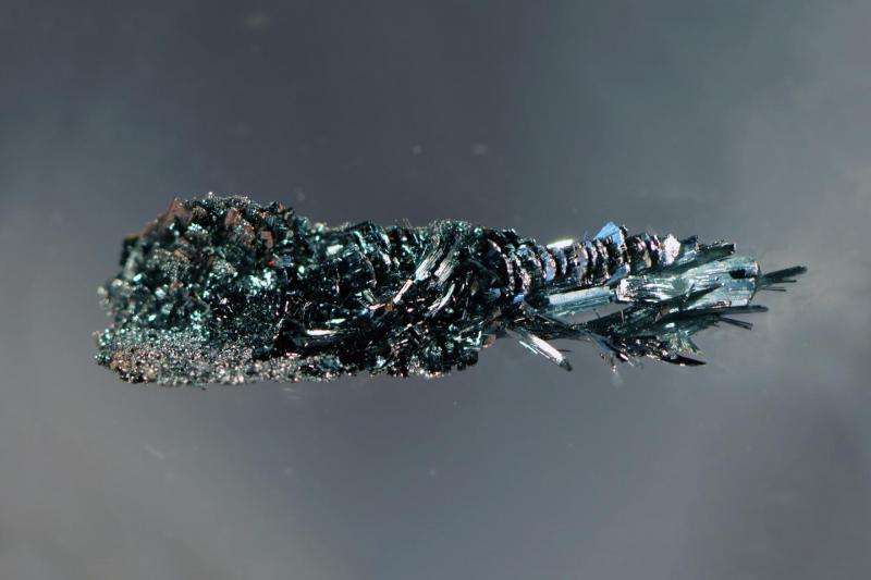
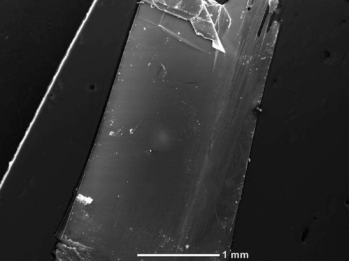
The demand for a silicon material aided the discovery of graphene, a single layer of graphite—which won the Nobel Prize in Physics in 2010. Since this time, scientists and engineers have developed many two-dimensional (2D) material innovations—layered materials with the thickness of only one atom or a few atoms. One such layered 2D material is black arsenic phosphorous. Now, a team of scientists at USC Viterbi, in collaboration with Technische Universität München, Germany, Universität Regensburg, Germany, and Yale University, have developed a new method to synthesize black arsenic-phosphorous without high pressure. This method demands less energy and is cheaper, and the synthesized materials have some incredible new properties.
The innovation, developed by USC Viterbi researchers, including Bilu Liu, the paper's lead author and postdoctoral researcher; Ahamad Abbas, graduate student; Han Wang, assistant professor; Rohan Dhall, graduate student; Stephen B. Cronin, associate professor; Mingyuan Ge, research assistant; Xin Fang, graduate student; and Professor Chongwu Zhou of the Ming Hsieh Department of Electrical Engineering, in concert with their collaborators, is documented in a paper titled "Black Arsenic-Phosphorus: Layered Anisotropic Infrared Semiconductors with Highly Tunable Compositions and Properties." The paper appeared in Advanced Materials on June 25, 2015.

What the researchers are most excited about is the ability to adjust the electronic and optical properties of these materials to a range that cannot be achieved by any other 2D materials thus far. This includes manipulating the materials' chemical compositions during materials synthesis and the materials' ability to sense long wavelength infrared (LWIR) waves due to their small energy gaps. This particular electromagnetic spectral range of LWIR is important for a range of applications such as LIDAR (light radar) systems, basically because LWIR waves are highly transparent in earth atmosphere. This wave range also has great application for the soldiers in the military who rely on infrared thermal imaging technology and for flexible night vision glasses. Another intriguing aspect of these new layered semiconductors is their anisotropic electronic and optical properties, which means the materials have different properties along x and y direction in the same plane. The researchers believe these are marked improvement from existing materials and devices and would lead to unique applications.
In addition, the researchers anticipate that it could also lead to important improvement for devices that monitor the environment. "We believe these materials are important members in a large family of 2D materials, because they fit into the long-wavelength-infrared light range and deliver properties that any other currently existing 2D materials cannot," said Zhou, the research team leader.
According to Liu, the paper's lead author: "As these are rather new materials, we anticipate there is lots of exciting fundamental physics research as well as engineering work to be done. For example, what's the electronic and optical properties of a truly single layer black arsenic phosphorus?"
More information: Liu, B., Köpf, M., Abbas, A. N., Wang, X., Guo, Q., Jia, Y., Xia, F., Weihrich, R., Bachhuber, F., Pielnhofer, F., Wang, H., Dhall, R., Cronin, S. B., Ge, M., Fang, X., Nilges, T. and Zhou, C. (2015), Black Arsenic–Phosphorus: Layered Anisotropic Infrared Semiconductors with Highly Tunable Compositions and Properties. Adv. Mater.. DOI: 10.1002/adma.201501758
Journal information: Advanced Materials
Provided by University of Southern California


