On-chip topological light: First measurements of transmission and delay

Topological transport of light is the photonic analog of topological electron flow in certain semiconductors. In the electron case, the current flows around the edge of the material but not through the bulk. It is "topological" in that even if electrons encounter impurities in the material the electrons will continue to flow without losing energy.
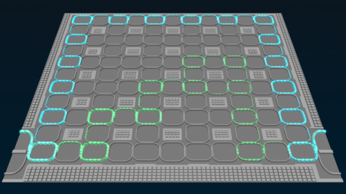
In the photonic equivalent, light flows not through and around a regular material but in a meta-material consisting of an array of tiny glass loops fabricated on a silicon substrate. If the loops are engineered just right, the topological feature appears: light sent into the array easily circulates around the edge with very little energy loss (even if some of the loops aren't working) while light taking an interior route suffers loss.
Mohammad Hafezi and his colleagues at the Joint Quantum Institute have published a series of papers on the subject of topological light. The first pointed out the potential application of robustness in delay lines and conceived a scheme to implement quantum Hall models in arrays of photonic loops. In photonics, signals sometimes need to be delayed, usually by sending light into a kilometers-long loop of optical fiber. In an on-chip scheme, such delays could be accomplished on the microscale; this is in addition to the energy-loss reduction made possible by topological robustness.
The next paper reported on results from an actual experiment. Since the tiny loops aren't perfect, they do allow a bit of light to escape vertically out of the plane of the array. This faint light allowed the JQI experimenters to image the course of light. This confirmed the plan that light persists when it goes around the edge of the array but suffers energy loss when traveling through the bulk.
The third paper, appearing now in Physical Review Letters, actually delivers detailed measurements of the transmission (how much energy is lost) and delay for edge-state light and for bulk-route light. The paper is notable enough to have received an "editor's suggestion" designation. "Apart from the potential photonic-chip applications of this scheme," said Hafezi, "this photonic platform could allow us to investigate fundamental quantum transport properties."

Another measured quality is consistency. Sunil Mittal, a graduate student at the University of Maryland and first author on the paper, points out that microchip manufacturing is not a perfect process. "Irregularities in integrated photonic device fabrication usually result in device-to-device performance variations," he said. And this usually undercuts the microchip performance. But with topological protection (photons traveling at the edge of the array are practically invulnerable to impurities) at work, consistency is greatly strengthened.
Indeed, the authors, reporting trials with numerous array samples, reveal that for light taking the bulk (interior) route in the array, the delay and transmission of light can vary a lot, whereas for light making the edge route, the amount of energy loss is regularly less and the time delay for signals more consistent. Robustness and consistency are vital if you want to integrate such arrays into photonic schemes for processing quantum information.
Discover the latest in science, tech, and space with over 100,000 subscribers who rely on Phys.org for daily insights. Sign up for our free newsletter and get updates on breakthroughs, innovations, and research that matter—daily or weekly.
How does the topological property emerge at the microscopic level? First, look at the electron topological behavior, which is an offshoot of the quantum Hall effect. Electrons, under the influence of an applied magnetic field can execute tiny cyclonic orbits. In some materials, called topological insulators, no external magnetic field is needed since the necessary field is supplied by spin-orbit interactions—-that is, the coupling between the orbital motion of electrons and their spins. In these materials the conduction regime is topological: the material is conductive around the edge but is an insulator in the interior.
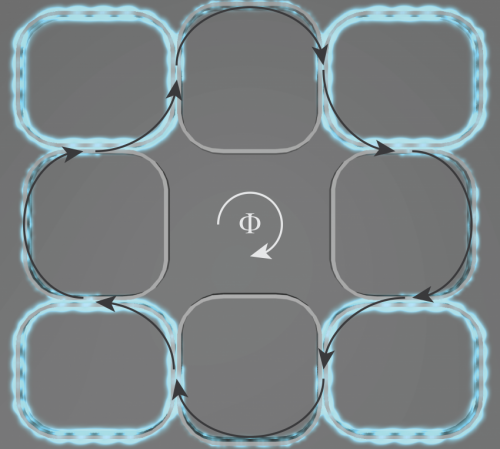
And now for the photonic equivalent. Light waves do not usually feel magnetic fields, and if they do it is very weak. In the photonic case, the equivalent of a magnetic field is supplied by a subtle phase shift imposed on the light as it circulates around the loops. Actually the loops in the array are of two kinds: resonator loops designed to exactly accommodate light at a certain frequency, allowing the waves to circle the loop many times. Link loops, by contrast, are not exactly suited to the waves, and are designed chiefly to pass the light onto the neighboring resonator loop.
Light that circulates around one unit cell of the loop array will undergo a slight phase change, an amount signified by the letter phi. That is, the light signal, in coming around the unit cell, re-arrives where it started advanced or retarded just a bit from its original condition. Just this amount of change imparts the topological robustness to the global transmission of the light in the array.
In summary, documented on-chip light delay and a robust, consistent, low-loss transport of light has now been demonstrated. The transport of light is tunable to a range of frequencies and the chip can be manufactured using standard micro-fabrications techniques.
More information: "Topologically Robust Transport of Photons in a Synthetic Gauge Field," S. Mittal, J. Fan, S. Faez, A. Migdall, J. M. Taylor, and M. Hafezi, Physical Review Letters, to be published in August 2014; archive version: arxiv.org/pdf/1404.0090v1.pdf
Journal information: Physical Review Letters
Provided by Joint Quantum Institute


